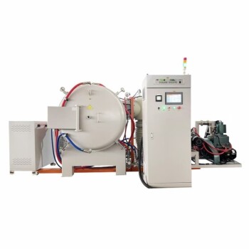
The primary objective of using Ultra-High Vacuum Chemical Vapor Deposition (UHVCVD) systems for TCO film preparation is to eliminate contamination from ambient gases by maintaining extremely low pressures, typically below $10^{-10}$ Pa. This ultra-clean environment enables precise, atomic-level management of the film’s growth, resulting in materials with exceptional purity and superior optoelectronic performance.
By removing interference from background gases, UHVCVD transforms film deposition from a bulk coating process into a precise engineering discipline. It allows you to define the material's microstructure and defect density at the fundamental atomic level.
The Critical Role of Extreme Vacuum
Eliminating Environmental Contamination
The defining characteristic of UHVCVD is its operating pressure, which drops below $10^{-10}$ Pa.
At this level of vacuum, the presence of ambient gases—such as oxygen or water vapor—is drastically reduced. This ensures that the chemical precursors react only with the substrate and each other, rather than with impurities floating in the chamber.
Enhancing Optoelectronic Performance
For Transparent Conductive Oxide (TCO) films, purity is directly linked to performance.
Contaminants act as scattering centers for electrons and photons, which degrades conductivity and transparency. By minimizing these impurities, UHVCVD produces films that function at the theoretical limits of their optoelectronic potential.
Engineering at the Atomic Scale
Precision Microstructure Control
UHVCVD does not simply deposit layers; it allows for the management of film microstructure.
Because the process is not disrupted by foreign particles, you can dictate exactly how the crystal lattice forms. This control extends to the film's thickness, ensuring uniformity that is difficult to achieve in higher-pressure environments.
Managing Defect Density
A major advantage of this high-purity environment is the reduction of structural defects.
Defects in the crystal structure often serve as trap states that impede electron flow. UHVCVD allows for the growth of films with significantly lower defect densities, yielding higher quality electronic materials.
Operational Considerations and Trade-offs
The Cost of Perfection
While UHVCVD offers superior quality, it requires rigorous system maintenance to sustain pressures below $10^{-10}$ Pa.
Achieving and maintaining this level of vacuum adds complexity to the equipment and the process cycle compared to standard CVD or atmospheric methods. It is a specialized approach reserved for applications where material fidelity is non-negotiable.
Making the Right Choice for Your Goal
When deciding whether to implement UHVCVD for your TCO film preparation, consider your specific performance requirements.
- If your primary focus is Maximum Optoelectronic Efficiency: Use UHVCVD to minimize electron scattering and maximize transparency by eliminating background gas impurities.
- If your primary focus is Microstructural Precision: Rely on UHVCVD to control film thickness and defect density at the atomic level, ensuring highly uniform material growth.
Ultimately, UHVCVD is the definitive choice when the quality of the material interface dictates the success of the device.
Summary Table:
| Feature | UHVCVD Advantage for TCO Films |
|---|---|
| Vacuum Level | Below $10^{-10}$ Pa (Ultra-High Vacuum) |
| Primary Objective | Eliminate contamination from ambient gases |
| Material Quality | Atomic-level purity and uniform microstructure |
| Key Benefit | Reduced defect density and electron scattering |
| Performance Impact | Maximum transparency and electrical conductivity |
Elevate Your Thin Film Research with KINTEK
Precision at the atomic level requires equipment engineered for perfection. KINTEK specializes in advanced laboratory solutions, offering a comprehensive range of high-performance systems including CVD, PECVD, and MPCVD units designed to meet the most rigorous vacuum and temperature requirements.
Whether you are developing next-generation Transparent Conductive Oxides or advancing battery research, our portfolio—from high-temperature furnaces and vacuum systems to isostatic presses and specialized consumables—provides the reliability your lab demands.
Ready to achieve theoretical limits in material performance? Contact our technical experts today to find the ideal solution for your thin film deposition and material processing needs.
References
- Wen He, Haowei Huang. Advancements in Transparent Conductive Oxides for Photoelectrochemical Applications. DOI: 10.3390/nano14070591
This article is also based on technical information from Kintek Solution Knowledge Base .
Related Products
- CVD Diamond Cutting Tool Blanks for Precision Machining
- Lab Blown Film Extrusion Three Layer Co-Extrusion Film Blowing Machine
- Graphite Vacuum Furnace High Thermal Conductivity Film Graphitization Furnace
- Graphite Vacuum Furnace Bottom Discharge Graphitization Furnace for Carbon Materials
- Vacuum Heat Treat and Sintering Furnace with 9MPa Air Pressure
People Also Ask
- What is the hardness of CVD diamond? The Ultimate Guide to Engineered Super-Materials
- What is the difference between metallic and non-metallic coating? A Guide to Sacrificial vs. Barrier Protection
- What is the carbon footprint of diamond mining? Uncovering the True Environmental and Ethical Cost
- What are 5 negative impacts of diamond mines on the environment? The Hidden Environmental Cost of Diamond Mining
- Why is diamond used for making or coating tool? Unlock Unmatched Hardness and Precision
