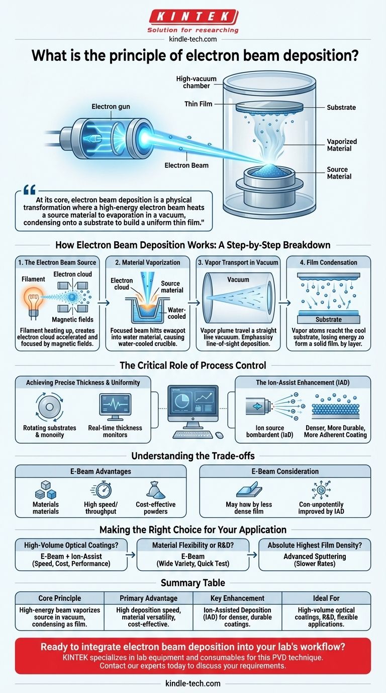
At its core, the principle of electron beam deposition is a process of physical transformation where a high-energy beam of electrons heats a source material to the point of evaporation. This vaporized material then travels through a vacuum and condenses onto a target object, or substrate, building up a highly uniform thin film. The entire process is managed by precise computer control over factors like vacuum level and deposition rate to achieve specific coating characteristics.
Electron beam deposition is a versatile Physical Vapor Deposition (PVD) technique valued for its speed and material flexibility. Its effectiveness hinges on transforming a solid source into a vapor using a focused electron beam, with final film quality being heavily influenced by process control and optional enhancements like ion assistance.
How Electron Beam Deposition Works: A Step-by-Step Breakdown
To understand its application, we must first break down the core physical process into its distinct stages. Each step is critical for forming a high-quality thin film.
The Electron Beam Source
The process begins in an electron gun, where a filament is heated to produce a cloud of electrons. These electrons are then accelerated by high voltage and focused into a tight beam using magnetic fields.
Material Vaporization
This high-energy electron beam is directed onto the source material, often held in a water-cooled copper crucible. The intense, localized energy from the electrons heats the material past its melting point and into its evaporation or sublimation point, creating a plume of vapor.
Vapor Transport in Vacuum
This entire operation takes place in a high-vacuum chamber. The vacuum is crucial because it removes air molecules, allowing the vaporized material to travel in a straight, unimpeded line from the source to the substrate. This is known as line-of-sight deposition.
Film Condensation
When the vapor atoms or molecules reach the relatively cool surface of the substrate (such as an optical lens or a semiconductor wafer), they lose energy and condense back into a solid state. This slow, controlled accumulation builds the thin film layer by layer.
The Critical Role of Process Control
Simply evaporating and condensing material is not enough. The true value of E-Beam deposition comes from the ability to precisely control the film's properties.
Achieving Precise Thickness and Uniformity
Computers meticulously control the power of the electron beam, which dictates the rate of evaporation. By rotating the substrates and monitoring film thickness in real-time, highly uniform coatings with pre-specified thicknesses can be achieved across multiple objects in a single batch.
The Ion-Assist Enhancement (IAD)
To improve the coating's physical properties, the process can be enhanced with an Ion-Assisted Deposition (IAD) system. A separate ion source bombards the substrate with low-energy ions as the film grows, which transfers extra energy to the condensing atoms. This results in a denser, more durable, and more adherent coating with reduced internal stress.
Understanding the Trade-offs
No single technique is perfect for every scenario. Electron beam deposition is chosen for specific advantages, but it's important to understand its context relative to other methods like magnetron sputtering.
Advantage: Material Versatility and Cost
E-Beam can evaporate a vast range of materials, including metals and dielectric compounds. This is a significant advantage over sputtering, which requires the source material to be fabricated into a specific and often expensive "target." E-Beam can use less expensive powders or granules directly.
Advantage: Deposition Speed
In batch scenarios, E-Beam deposition is often much faster than sputtering. This higher throughput makes it exceptionally well-suited for high-volume commercial applications, particularly in the optics industry.
Consideration: Film Density and Adhesion
A standard E-Beam process may produce films that are less dense than those produced by sputtering. This is the primary reason Ion-Assisted Deposition is so frequently paired with E-Beam. IAD effectively closes this performance gap, allowing E-Beam to deliver both speed and high-quality film structure.
Making the Right Choice for Your Application
Selecting a deposition method requires aligning the process capabilities with your project's end goal.
- If your primary focus is high-volume optical coatings: E-Beam with ion-assist is an industry standard, offering an excellent balance of speed, cost, and high-performance film properties.
- If your primary focus is material flexibility or R&D: E-Beam provides the ability to quickly test and deposit a wide variety of materials without the high cost and lead time of sourcing custom sputter targets.
- If your primary focus is the absolute highest film density without an assist source: Some advanced sputtering techniques may hold an edge, but they typically come at the cost of slower deposition rates and more limited material options.
Ultimately, understanding the principle of E-Beam deposition reveals it as a powerful and adaptable tool for creating advanced thin films.
Summary Table:
| Key Aspect | Description |
|---|---|
| Core Principle | A high-energy electron beam vaporizes a source material in a vacuum, which then condenses on a substrate to form a thin film. |
| Primary Advantage | High deposition speed and material versatility, using cost-effective powders or granules. |
| Key Enhancement | Ion-Assisted Deposition (IAD) can be used to create denser, more durable coatings. |
| Ideal For | High-volume optical coatings, R&D, and applications requiring material flexibility. |
Ready to integrate electron beam deposition into your lab's workflow? KINTEK specializes in providing the lab equipment and consumables you need to leverage this versatile PVD technique. Whether you're scaling up optical coating production or conducting advanced materials R&D, our solutions help you achieve precise, high-quality thin films efficiently. Contact our experts today to discuss how we can support your specific laboratory requirements.
Visual Guide
Related Products
- Electron Beam Evaporation Coating Oxygen-Free Copper Crucible and Evaporation Boat
- RF PECVD System Radio Frequency Plasma-Enhanced Chemical Vapor Deposition RF PECVD
- Electron Beam Evaporation Coating Tungsten Crucible and Molybdenum Crucible for High Temperature Applications
- Electron Beam Evaporation Coating Conductive Boron Nitride Crucible BN Crucible
- Electron Beam Evaporation Coating Gold Plating Tungsten Molybdenum Crucible for Evaporation
People Also Ask
- What is e-beam evaporation? Achieve High-Purity Thin Film Deposition for Your Lab
- What is e-beam evaporation used for? Precision Coating for Optics, Aerospace & Electronics
- What is the deposition rate of e-beam evaporation? Control Thin Film Quality and Speed
- What is the current of e-beam evaporation? A Guide to High-Purity Thin Film Deposition
- What is the temperature of e-beam evaporation? Mastering the Two-Zone Thermal Process for Precision Films


