In essence, electron beam physical vapor deposition (EBPVD) is a high-vacuum process used to create exceptionally pure and precise thin films. It works by using a magnetically focused, high-energy beam of electrons to melt and vaporize a source material. This material vapor then travels through the vacuum and condenses onto a substrate, forming the desired coating layer by layer.
The central takeaway is that EBPVD is not simply a heating method; it is a highly controlled technique for vaporizing materials with extreme precision. Its primary advantage lies in its ability to efficiently coat substrates with materials that have very high melting points, achieving a level of purity and density that other methods struggle to match.
The Core Mechanics of EBPVD
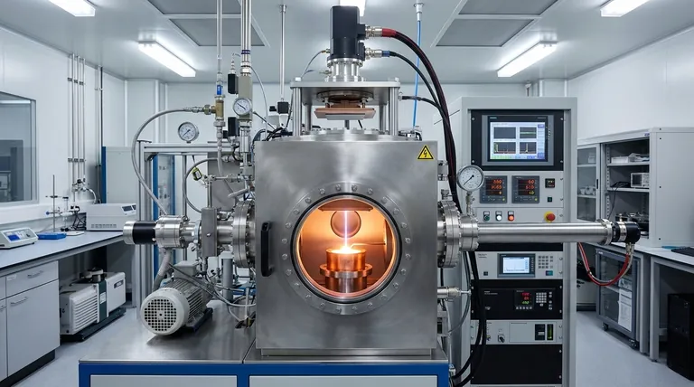
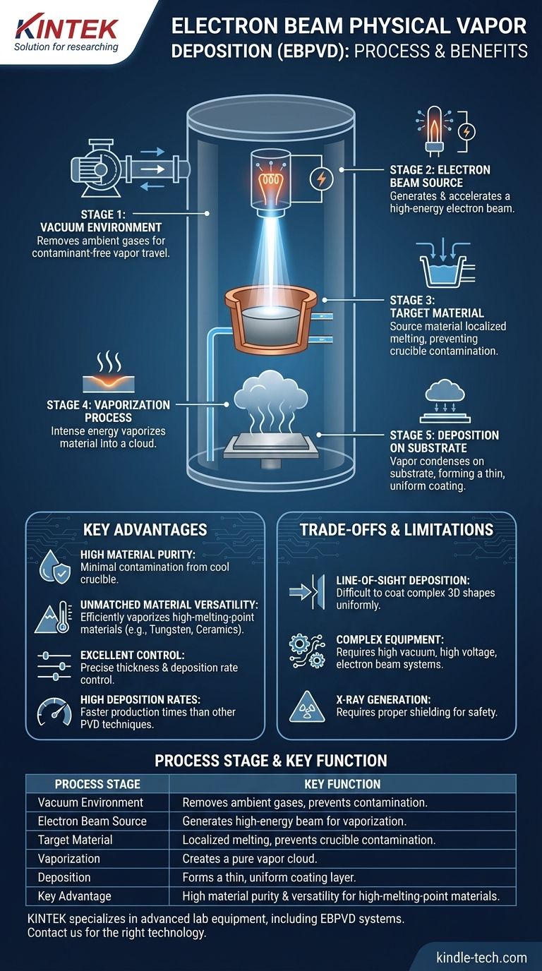
To understand EBPVD, it's best to break it down into its fundamental stages, each occurring within a high-vacuum chamber. This environment is critical for preventing contamination and ensuring the vaporized material can travel unimpeded.
The Vacuum Environment
First, the entire process takes place in a chamber pumped down to a high vacuum. This removes ambient gases like oxygen and nitrogen, which could otherwise react with the vaporized material and introduce impurities into the final film.
The Electron Beam Source
A filament, typically made of tungsten, is heated to a high temperature, causing it to emit a stream of electrons. These electrons are then accelerated by a high-voltage power supply, forming a high-energy beam.
The Target Material
The source material to be deposited—often in the form of powder, granules, or a solid ingot—is placed in a water-cooled copper crucible. This cooling is crucial, as it ensures only the top surface of the material is melted by the electron beam, preventing contamination from the crucible itself.
The Vaporization Process
Magnetic fields are used to precisely steer and focus the electron beam onto the surface of the source material. The intense kinetic energy of the electrons is instantly converted to thermal energy upon impact, causing the material to rapidly heat, melt, and then evaporate, creating a vapor cloud.
The Deposition on the Substrate
The vaporized atoms travel in a straight line from the source toward the substrate (the object to be coated), which is positioned above. Upon hitting the cooler surface of the substrate, the vapor condenses back into a solid state, forming a thin, uniform film.
Precision Control and Enhancement
The thickness of the deposited film is meticulously controlled by computer systems that monitor the deposition rate in real time. For even denser and more robust coatings, the process can be enhanced with an ion beam, which bombards the substrate during deposition to increase adhesion and reduce stress in the film.
Why Choose EBPVD? Key Advantages
EBPVD is a preferred method in many advanced industries, particularly for optics, aerospace, and semiconductors, due to several distinct advantages.
High Material Purity
Because the electron beam only heats the source material and the crucible remains cool, there is minimal contamination. This results in coatings of exceptionally high purity.
Unmatched Material Versatility
The electron beam can generate extremely high localized temperatures. This makes EBPVD one of the few methods capable of efficiently vaporizing materials with very high melting points, such as titanium, tungsten, and various ceramics.
Excellent Control Over Thickness
The process allows for precise, real-time control over the deposition rate and final film thickness, which is critical for applications like optical filters and semiconductor devices.
High Deposition Rates
Compared to other PVD techniques like sputtering, EBPVD can often achieve much higher deposition rates, leading to faster production times.
Understanding the Trade-offs and Limitations
No technology is without its compromises. A clear-eyed view of EBPVD requires acknowledging its specific challenges.
Line-of-Sight Deposition
The vaporized material travels in straight lines. This means it can be difficult to uniformly coat complex, three-dimensional shapes with undercuts or hidden surfaces without sophisticated substrate rotation and tilting mechanisms.
Complex and Expensive Equipment
The need for a high-vacuum environment, high-voltage power supplies, and electron beam steering systems makes EBPVD equipment more complex and costly than some alternative methods.
Potential for X-Ray Generation
The impact of high-energy electrons on the target material can generate X-rays. This requires proper shielding of the vacuum chamber to ensure operator safety, adding to the system's complexity.
Making the Right Choice for Your Application
Selecting the right deposition technology depends entirely on your project's specific goals.
- If your primary focus is ultimate purity and depositing high-melting-point materials: EBPVD is the superior choice for creating high-performance optical coatings, thermal barriers on turbine blades, or conductive layers in advanced electronics.
- If your primary focus is coating complex 3D geometries uniformly: You may need to consider a non-line-of-sight process like Chemical Vapor Deposition (CVD), which uses a chemical reaction to deposit a film.
- If your primary focus is cost-effective deposition of common metals: A simpler PVD technique like sputtering might offer a better balance of performance and cost for less demanding applications.
Ultimately, understanding these core principles empowers you to select the right deposition technology not just based on the material, but on the specific outcome you need to achieve.
Summary Table:
| Process Stage | Key Function | Outcome |
|---|---|---|
| Vacuum Environment | Removes ambient gases | Prevents contamination, ensures clean vapor travel |
| Electron Beam Source | Generates & accelerates electrons | Creates high-energy beam for vaporization |
| Target Material | Source material in cooled crucible | Localized melting, prevents crucible contamination |
| Vaporization | Electron beam melts/vaporizes material | Creates a pure vapor cloud |
| Deposition | Vapor condenses on substrate | Forms a thin, uniform coating layer |
| Key Advantage | High material purity & versatility | Ideal for high-melting-point materials like ceramics and metals |
Need a high-purity coating solution for your lab?
Electron Beam PVD is essential for applications demanding the highest levels of material purity and the ability to work with challenging, high-melting-point materials. If your work in optics, aerospace, or semiconductor manufacturing requires precise, dense, and contaminant-free thin films, EBPVD is the superior choice.
KINTEK specializes in advanced lab equipment, including deposition systems tailored for rigorous research and production needs. Let our experts help you determine if EBPVD is the right technology for your specific application. We provide the equipment and support to ensure your lab achieves exceptional results.
Contact our team today to discuss your project requirements and discover the right coating solution for you.
Visual Guide
Related Products
- Electron Beam Evaporation Coating Oxygen-Free Copper Crucible and Evaporation Boat
- RF PECVD System Radio Frequency Plasma-Enhanced Chemical Vapor Deposition RF PECVD
- Electron Beam Evaporation Coating Gold Plating Tungsten Molybdenum Crucible for Evaporation
- Electron Beam Evaporation Coating Tungsten Crucible and Molybdenum Crucible for High Temperature Applications
- Chemical Vapor Deposition CVD Equipment System Chamber Slide PECVD Tube Furnace with Liquid Gasifier PECVD Machine
People Also Ask
- What is the voltage of e-beam evaporation? Achieve Precise Thin-Film Deposition
- What is the current of e-beam evaporation? A Guide to High-Purity Thin Film Deposition
- What is e-beam evaporation used for? Precision Coating for Optics, Aerospace & Electronics
- What is the deposition rate of e-beam evaporation? Control Thin Film Quality and Speed
- What is the container that holds the metal source material called in e-beam evaporation? Ensure Purity and Quality in Your Thin-Film Deposition


