In nanotechnology, MOCVD is a highly controlled chemical construction process used to grow ultra-thin, high-purity crystalline films. It works by introducing specific metal-organic precursor gases into a reaction chamber where they decompose on a heated substrate, chemically reacting to form a solid layer of material one atomic layer at a time. This method is a cornerstone for fabricating advanced semiconductor devices.
At its core, Metal-Organic Chemical Vapor Deposition (MOCVD) is not a physical coating process but a precise chemical reaction. It leverages carefully controlled gas flows, temperature, and pressure to build complex nanostructures, like quantum wells, from the bottom up on a crystalline foundation.
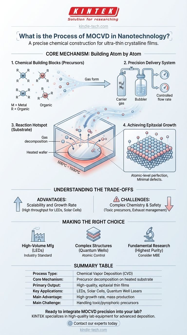
The Core Mechanism: Building Atom by Atom
MOCVD is fundamentally a process of delivering chemical ingredients in the gas phase to a specific location where they react to form a solid. Each step is engineered for maximum precision, enabling the construction of materials with features measured in nanometers.
The Chemical Building Blocks (Precursors)
The process begins with the selection of metal-organic precursors. These are complex molecules that contain the desired metal atom (like gallium, indium, or aluminum) bonded to organic groups.
These precursors are chosen because they are volatile, meaning they can be easily turned into a gas at relatively low temperatures. This allows them to be transported into the reaction chamber.
The Precision Delivery System
To control the amount of precursor entering the chamber, a carrier gas (like hydrogen or nitrogen) is bubbled through the liquid metal-organic source. This is often called a bubbler system.
By precisely controlling the temperature of the bubbler and the flow rate of the carrier gas, engineers can determine the exact concentration of the precursor in the gas stream, which directly influences the growth rate of the film.
The Reaction Hotspot (The Substrate)
The mixed gases flow over a heated wafer, known as the substrate. This substrate, heated to temperatures between 500°C and 1500°C, acts as the catalyst and foundation for the new material.
The intense heat breaks down the precursor molecules, releasing the metal atoms which then react with other gases (like arsine or phosphine for compound semiconductors) on the substrate surface. This chemical reaction forms the desired solid, crystalline film.
Achieving Epitaxial Growth
The result of this controlled reaction is typically a high-quality epitaxial film. This means the new crystalline layer grows in perfect alignment with the crystal structure of the underlying substrate.
This atomic-level perfection is critical for the performance of nano-electronic and optoelectronic devices, as it minimizes defects that would otherwise disrupt the flow of electrons or photons.
Understanding the Trade-offs
While powerful, MOCVD is a complex process with inherent advantages and challenges that dictate its suitability for a given application. It's a balance of speed, complexity, and purity.
Advantage: Scalability and Growth Rate
Compared to ultra-high vacuum techniques like Molecular Beam Epitaxy (MBE), MOCVD generally offers higher growth rates. This makes it more suitable for high-volume manufacturing of devices like LEDs and solar cells.
Challenge: Complex Chemistry
The chemical reactions in MOCVD are intricate and can produce unwanted by-products. The precursors themselves are often highly toxic and pyrophoric (ignite spontaneously in air), requiring sophisticated safety and handling protocols.
Challenge: By-product Removal
All unreacted precursor gases and chemical by-products must be safely and completely removed from the reaction chamber. This exhaust management is a critical part of the system design and operation.
Making the Right Choice for Your Goal
Selecting MOCVD depends entirely on the requirements for material quality, production volume, and the complexity of the desired nanostructure.
- If your primary focus is high-volume manufacturing of optoelectronics (like LEDs): MOCVD is the industry standard due to its higher throughput and excellent control over compound semiconductor alloys.
- If your primary focus is creating complex, multi-layered quantum structures: MOCVD provides the atomic-level thickness and composition control needed to build these advanced heterostructures.
- If your primary focus is fundamental research requiring the absolute highest material purity: You may need to consider alternative methods like MBE, which operates in a cleaner vacuum environment but at a slower pace.
Ultimately, MOCVD is a foundational manufacturing technique that translates chemical precision into the nanoscale devices that power our modern world.
Summary Table:
| Aspect | Key Details |
|---|---|
| Process Type | Chemical Vapor Deposition (CVD) |
| Core Mechanism | Precursor gases decompose on a heated substrate |
| Primary Output | High-quality, epitaxial thin films |
| Key Applications | LEDs, Solar Cells, Quantum Well Lasers |
| Main Advantage | High growth rate, suitable for mass production |
| Main Challenge | Handling of toxic and pyrophoric precursors |
Ready to integrate MOCVD precision into your lab's capabilities?
KINTEK specializes in providing high-quality lab equipment and consumables for advanced material deposition processes like MOCVD. Whether you are scaling up production of optoelectronic devices or pushing the boundaries of nanomaterial research, our expertise and reliable products support your innovation.
Contact our experts today to discuss how our solutions can enhance your nanotechnology workflows and help you achieve superior film quality and process control.
Visual Guide
Related Products
- Multi Heating Zones CVD Tube Furnace Machine Chemical Vapor Deposition Chamber System Equipment
- 915MHz MPCVD Diamond Machine Microwave Plasma Chemical Vapor Deposition System Reactor
- Microwave Plasma Chemical Vapor Deposition MPCVD Machine System Reactor for Lab and Diamond Growth
- Cylindrical Resonator MPCVD Machine System Reactor for Microwave Plasma Chemical Vapor Deposition and Lab Diamond Growth
- Molybdenum Vacuum Heat Treat Furnace
People Also Ask
- What is the difference between hot wall CVD and cold wall CVD? Choose the Right System for Your Process
- What are the differences between chemical vapour deposition processes? A Guide to Pressure, Quality & Cost
- What are the advantages of using a Multi-zone Tube Furnace? Enhanced Thermal Uniformity for Diffusion Research
- How is graphene synthesized? Choosing the Right Method for Your Application
- What is the function of a tube furnace in CVD SiC synthesis? Achieving Ultra-Pure Silicon Carbide Powders