Knowledge What is the purpose of adding a boron source in CVD diamond growth? Master P-Type Semiconductor Conductivity
Author avatar

Tech Team · Kintek Solution

Updated 4 hours ago

What is the purpose of adding a boron source in CVD diamond growth? Master P-Type Semiconductor Conductivity


The primary purpose of introducing a boron source, such as trimethylboron, during Chemical Vapor Deposition (CVD) is to fundamentally alter the diamond's electrical properties. By causing boron atoms to substitute carbon atoms within the lattice structure, the material transforms from a natural electrical insulator into a conductive p-type semiconductor.

While natural diamond is renowned for being electrically insulating, the strategic addition of boron allows for the creation of Boron-Doped Diamond (BDD). This modification unlocks critical industrial capabilities, specifically chemical stability and electrochemical conductivity, that pure diamond cannot offer.

The Mechanics of Modification

Atomic Substitution

The fundamental principle of CVD is the atomic-level growth of a diamond. In a standard process, pure carbon atoms from a gas source bond with a diamond seed crystal, stacking layer by layer.

When a boron source is introduced, boron atoms integrate directly into this growing lattice. They replace carbon atoms, effectively "doping" the material.

The CVD Environment

This substitution occurs within a sealed chamber under specific conditions. The process typically requires low pressures (below 27 kPa) and temperatures around 800 to 1000 degrees Celsius.

Energy sources like microwaves or lasers ionize carbon-rich gases (such as methane) and the boron source into plasma. This breaks down molecular bonds, allowing the boron and carbon to co-deposit onto the substrate.

Why Conductivity Matters

Creating a p-type Semiconductor

The most immediate result of this process is the creation of a p-type semiconductor.

Pure diamond resists the flow of electricity. By incorporating boron, you introduce charge carriers (holes) into the valence band, allowing the material to conduct electricity efficiently.

Unlocking Electrochemical Properties

Boron-Doped Diamond (BDD) electrodes possess a wide electrochemical window.

This property allows the material to withstand higher voltages in solution without breaking down the water (electrolysis) compared to other electrode materials.

Chemical Stability

BDD electrodes maintain the inherent robustness of diamond. They exhibit exceptional resistance to chemical corrosion, ensuring longevity even in harsh operating environments.

Understanding the Trade-offs

Purity vs. Functionality

Standard CVD processes aim for pure carbon deposition to grow high-quality single crystals.

Adding a boron source is an intentional introduction of impurities. While this degrades the optical purity and insulating nature of the diamond, it is a necessary trade-off to achieve electrical functionality.

Specificity of Application

This modification is strictly for functional applications. If the goal is to utilize diamond's thermal conductivity without electrical conductivity, or to achieve optical transparency, boron doping would be detrimental to the project.

Making the Right Choice for Your Goal

Whether you should introduce a boron source depends entirely on the intended application of the final diamond film.

  • If your primary focus is electrochemical applications: Incorporate a boron source to create BDD electrodes suitable for advanced oxidation processes, such as industrial wastewater treatment.
  • If your primary focus is optical or gem-quality growth: Exclude boron sources to ensure the lattice remains comprised of pure carbon atoms, maintaining the diamond's natural insulating and transparent properties.

By mastering the inclusion of boron, you transition diamond from a passive insulator to an active, industrial-grade electronic component.

Summary Table:

Feature Pure CVD Diamond Boron-Doped Diamond (BDD)
Electrical State Insulator p-type Semiconductor
Lattice Structure Pure Carbon Boron-substituted Carbon
Key Property Optical Transparency Electrochemical Conductivity
Electrochemical Window N/A Very Wide
Primary Application Optics, Thermal Management Wastewater Treatment, Electrodes

Elevate Your Electrochemical Research with KINTEK BDD Solutions

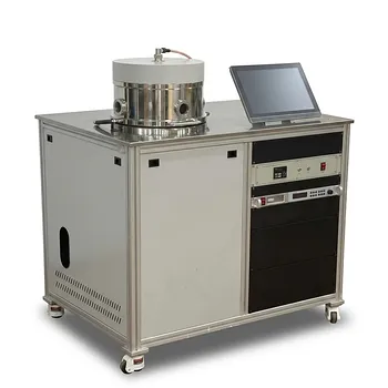
Transform your laboratory's capabilities with KINTEK’s high-precision equipment. Whether you are developing Boron-Doped Diamond (BDD) films for industrial wastewater treatment or advancing semiconductor research, our comprehensive range of CVD systems (including PECVD and MPCVD) and high-temperature reactors provides the precision control required for atomic substitution.

Why choose KINTEK?

  • Advanced Coating Technology: Perfect your boron-doping process with our high-performance plasma chambers.
  • Comprehensive Lab Portfolio: From electrolytic cells and electrodes to high-temperature furnaces and ceramic consumables, we support every stage of your material synthesis.
  • Expert Engineering: Our tools are designed for the extreme chemical stability and wide electrochemical windows required by target customers in the energy and environmental sectors.

Ready to achieve superior conductivity in your diamond growth? Contact KINTEK today for a customized quote!

References

  1. Roland Haubner. Low-pressure diamond: from the unbelievable to technical products. DOI: 10.1007/s40828-021-00136-z

This article is also based on technical information from Kintek Solution Knowledge Base .

Related Products

People Also Ask

Related Products

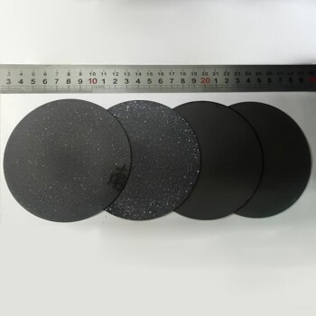
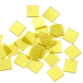
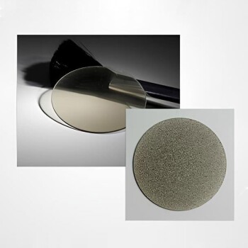
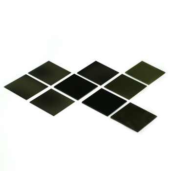
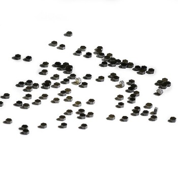
Laboratory CVD Boron Doped Diamond Materials

Laboratory CVD Boron Doped Diamond Materials

CVD boron-doped diamond: A versatile material enabling tailored electrical conductivity, optical transparency, and exceptional thermal properties for applications in electronics, optics, sensing, and quantum technologies.

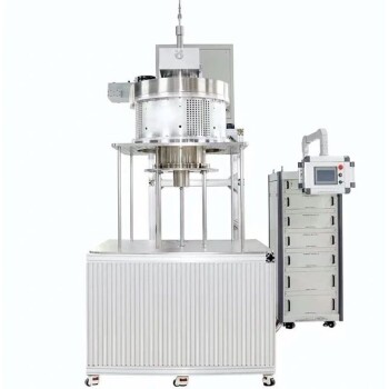
915MHz MPCVD Diamond Machine Microwave Plasma Chemical Vapor Deposition System Reactor

915MHz MPCVD Diamond Machine Microwave Plasma Chemical Vapor Deposition System Reactor

915MHz MPCVD Diamond Machine and its multi-crystal effective growth, the maximum area can reach 8 inches, the maximum effective growth area of single crystal can reach 5 inches. This equipment is mainly used for the production of large-size polycrystalline diamond films, the growth of long single crystal diamonds, the low-temperature growth of high-quality graphene, and other materials that require energy provided by microwave plasma for growth.

CVD Diamond Domes for Industrial and Scientific Applications

CVD Diamond Domes for Industrial and Scientific Applications

Discover CVD diamond domes, the ultimate solution for high-performance loudspeakers. Made with DC Arc Plasma Jet technology, these domes deliver exceptional sound quality, durability, and power handling.

Customer Made Versatile CVD Tube Furnace Chemical Vapor Deposition Chamber System Equipment

Customer Made Versatile CVD Tube Furnace Chemical Vapor Deposition Chamber System Equipment

Get your exclusive CVD furnace with KT-CTF16 Customer Made Versatile Furnace. Customizable sliding, rotating, and tilting functions for precise reactions. Order now!

CVD Diamond Cutting Tool Blanks for Precision Machining

CVD Diamond Cutting Tool Blanks for Precision Machining

CVD Diamond Cutting Tools: Superior Wear Resistance, Low Friction, High Thermal Conductivity for Non-Ferrous Materials, Ceramics, Composites Machining

HFCVD Machine System Equipment for Drawing Die Nano-Diamond Coating

HFCVD Machine System Equipment for Drawing Die Nano-Diamond Coating

The nano-diamond composite coating drawing die uses cemented carbide (WC-Co) as the substrate, and uses the chemical vapor phase method ( CVD method for short ) to coat the conventional diamond and nano-diamond composite coating on the surface of the inner hole of the mold.

Multi Heating Zones CVD Tube Furnace Machine Chemical Vapor Deposition Chamber System Equipment

Multi Heating Zones CVD Tube Furnace Machine Chemical Vapor Deposition Chamber System Equipment

KT-CTF14 Multi Heating Zones CVD Furnace - Precise Temperature Control and Gas Flow for Advanced Applications. Max temp up to 1200℃, 4 channels MFC mass flow meter, and 7" TFT touch screen controller.

Inclined Rotary Plasma Enhanced Chemical Vapor Deposition PECVD Equipment Tube Furnace Machine

Inclined Rotary Plasma Enhanced Chemical Vapor Deposition PECVD Equipment Tube Furnace Machine

Upgrade your coating process with PECVD coating equipment. Ideal for LED, power semiconductors, MEMS and more. Deposits high-quality solid films at low temps.

Split Chamber CVD Tube Furnace with Vacuum Station Chemical Vapor Deposition System Equipment Machine

Split Chamber CVD Tube Furnace with Vacuum Station Chemical Vapor Deposition System Equipment Machine

Efficient split chamber CVD furnace with vacuum station for intuitive sample checking and quick cooling. Up to 1200℃ max temperature with accurate MFC mass flowmeter control.

RF PECVD System Radio Frequency Plasma-Enhanced Chemical Vapor Deposition RF PECVD

RF PECVD System Radio Frequency Plasma-Enhanced Chemical Vapor Deposition RF PECVD

RF-PECVD is an acronym for "Radio Frequency Plasma-Enhanced Chemical Vapor Deposition." It deposits DLC (Diamond-like carbon film) on germanium and silicon substrates. It is utilized in the 3-12um infrared wavelength range.

Variable Speed Peristaltic Pump

Variable Speed Peristaltic Pump

KT-VSP Series Smart Variable Speed Peristaltic Pumps offer precise flow control for labs, medical, and industrial applications. Reliable, contamination-free liquid transfer.

1200℃ Split Tube Furnace with Quartz Tube Laboratory Tubular Furnace

1200℃ Split Tube Furnace with Quartz Tube Laboratory Tubular Furnace

KT-TF12 split tube furnace: high-purity insulation, embedded heating wire coils, and max. 1200C. Widely used for new materials and chemical vapour deposition.

Custom PTFE Teflon Parts Manufacturer for Non-Standard Insulator Customization

Custom PTFE Teflon Parts Manufacturer for Non-Standard Insulator Customization

PTFE insulator PTFE has excellent electrical insulation properties in a wide temperature and frequency range.

Glassy Carbon Sheet RVC for Electrochemical Experiments

Glassy Carbon Sheet RVC for Electrochemical Experiments

Discover our Glassy Carbon Sheet - RVC. Perfect for your experiments, this high-quality material will elevate your research to the next level.

Cylindrical Press Mold with Scale for Lab

Cylindrical Press Mold with Scale for Lab

Discover precision with our Cylindrical Press Mold. Ideal for high-pressure applications, it molds various shapes and sizes, ensuring stability and uniformity. Perfect for lab use.

Custom PTFE Teflon Parts Manufacturer for Acid and Alkali Resistant Chemical Powder Material Scoops

Custom PTFE Teflon Parts Manufacturer for Acid and Alkali Resistant Chemical Powder Material Scoops

Known for its excellent thermal stability, chemical resistance and electrical insulating properties, PTFE is a versatile thermoplastic material.

Custom PTFE Teflon Parts Manufacturer for Centrifuge Tube Racks

Custom PTFE Teflon Parts Manufacturer for Centrifuge Tube Racks

The precision-made PTFE test tube racks are completely inert and, due to the high temperature properties of PTFE, these test tube racks can be sterilized (autoclaved) without any problems.

Molybdenum Disilicide (MoSi2) Thermal Elements Electric Furnace Heating Element

Molybdenum Disilicide (MoSi2) Thermal Elements Electric Furnace Heating Element

Discover the power of Molybdenum Disilicide (MoSi2) Heating Element for high-temperature resistance. Unique oxidation resistance with stable resistance value. Learn more about its benefits now!

XRF & KBR plastic ring lab Powder Pellet Pressing Mold for FTIR

XRF & KBR plastic ring lab Powder Pellet Pressing Mold for FTIR

Get precise XRF samples with our plastic ring lab powder pellet pressing mold. Fast tableting speed and customizable sizes for perfect molding every time.


Leave Your Message