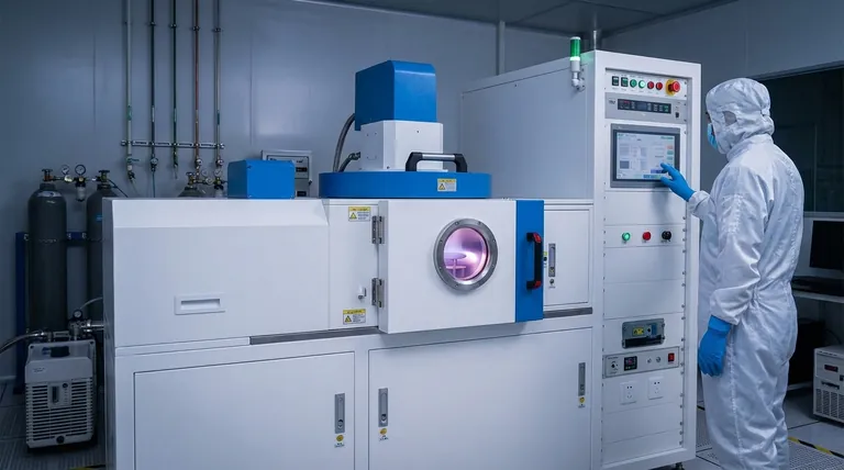
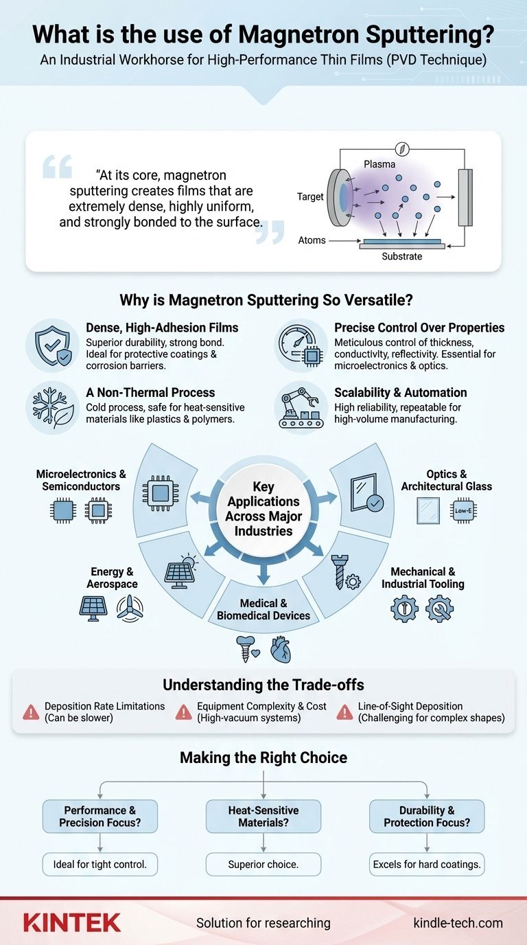
At its core, magnetron sputtering is an industrial workhorse for creating high-performance thin films. It is a physical vapor deposition (PVD) technique used to coat a vast range of materials, or substrates, with a thin layer of another material. These coatings are applied to alter the substrate's properties, enabling applications from microchips and solar panels to wear-resistant tools and medical implants.
The true value of magnetron sputtering lies not just in the wide array of coatings it can produce, but in its ability to do so with exceptional control. It allows for the creation of films that are extremely dense, highly uniform, and strongly bonded to the surface, making it the preferred method when coating quality and performance are critical.
The Foundation: Why is Magnetron Sputtering So Versatile?
The widespread adoption of magnetron sputtering is due to a few fundamental capabilities that make it uniquely suited for demanding industrial applications. It offers a level of precision and quality that other methods often cannot match on a large scale.
Creating Dense, High-Adhesion Films
One of the most significant advantages of sputtering is the high kinetic energy of the deposited atoms. This energy results in films that are incredibly dense and adhere strongly to the substrate.
This makes it ideal for protective applications, such as creating vapor barriers or corrosion-resistant layers that must withstand harsh environments.
Precise Control Over Film Properties
Magnetron sputtering allows for meticulous control over a film's thickness, composition, and structure. This precision is essential for tuning a material's functional characteristics.
Engineers can fine-tune a coating’s electrical conductivity, optical reflectivity or transparency, and even its magnetic properties. This is why it's critical for producing semi-transparent films on architectural glass and conductive layers in integrated circuits.
A Non-Thermal Coating Process
Unlike some deposition methods that rely on high heat to evaporate material, magnetron sputtering is a non-thermal, or "cold," process.
This is a crucial advantage for coating heat-sensitive materials like plastics, polymers, and delicate electronic components that would be damaged or destroyed by high-temperature techniques.
Scalability and Automation
The process is highly reliable and repeatable, making it perfect for high-volume manufacturing where consistency is key.
Magnetron sputtering systems are well-suited for automation, which is why they are a cornerstone of industries like semiconductor and hard disk manufacturing that require high throughput and minimal defects.
Key Applications Across Major Industries
The combination of control, quality, and versatility has made magnetron sputtering indispensable across numerous high-tech fields.
Microelectronics and Semiconductors
This is a primary use case. Sputtering is used to deposit the thin metallic and insulating layers that form the intricate circuitry within microchips, computer processors, and memory devices. It is also used in the manufacturing of flat-panel displays.
Optics and Architectural Glass
The technology is used to apply multi-layer coatings to glass that can reflect infrared radiation (heat) while allowing visible light to pass through. This is the basis for low-emissivity (Low-E) glass used in energy-efficient buildings. It's also used for anti-reflection coatings and decorative finishes.
Mechanical and Industrial Tooling
For the machining industry, sputtering creates super-hard, wear-resistant, and low-friction coatings on cutting tools, drills, and industrial components. These coatings dramatically extend the life and improve the performance of the tools.
Medical and Biomedical Devices
The biocompatibility and durability of sputtered films are critical in medicine. Applications include creating anti-rejection coatings on implants, conductive layers on angioplasty devices, and durable surfaces for dental implants.
Energy and Aerospace
In the energy sector, magnetron sputtering is used to deposit the functional layers in solar cells. In aerospace, it provides protective coatings for components like gas turbine blades and is used to deposit lightweight, functional films on magnesium alloys.
Understanding the Trade-offs
While powerful, magnetron sputtering is not the universal solution for every coating need. Understanding its limitations is key to making an informed decision.
Deposition Rate Limitations
Compared to simpler methods like thermal evaporation, magnetron sputtering can be a slower process. For applications where a thick coating is needed quickly and precision is less critical, other methods might be more cost-effective.
Equipment Complexity and Cost
Sputtering systems involve high-vacuum chambers, powerful magnets, and sophisticated power supplies. This represents a significant capital investment and requires specialized knowledge to operate and maintain effectively.
Line-of-Sight Deposition
Sputtering is a "line-of-sight" process, meaning the coating material travels in a straight line from the source (target) to the substrate. This can make it challenging to uniformly coat complex, three-dimensional shapes without advanced substrate rotation and manipulation systems.
Making the Right Choice for Your Goal
Deciding whether magnetron sputtering is the correct approach depends entirely on the specific requirements of your final product.
- If your primary focus is performance and precision: Magnetron sputtering is ideal for creating dense, uniform films where properties like electrical conductivity or optical transparency must be tightly controlled.
- If your primary focus is coating heat-sensitive materials: Its non-thermal nature makes it a superior choice for depositing high-quality films on plastics, polymers, and other delicate components.
- If your primary focus is durability and protection: The technology excels at producing hard, wear-resistant, and corrosion-resistant coatings that form an exceptionally strong bond with the substrate.
Ultimately, magnetron sputtering is the go-to industrial process when the performance, quality, and precision of a thin film are non-negotiable.
Summary Table:
| Key Advantage | Primary Benefit | Ideal Application |
|---|---|---|
| Dense, High-Adhesion Films | Superior durability and strong bond to substrate | Protective coatings, corrosion barriers |
| Precise Control | Tunable electrical, optical, and magnetic properties | Microelectronics, architectural glass |
| Non-Thermal Process | Safe for heat-sensitive materials (plastics, polymers) | Medical devices, delicate electronics |
| Scalability & Automation | High-volume, consistent manufacturing | Semiconductor production, hard disk drives |
Ready to elevate your product with high-performance thin films? KINTEK specializes in advanced lab equipment and consumables for magnetron sputtering, serving industries from microelectronics to medical devices. Our solutions deliver the precision, durability, and scalability your laboratory demands. Contact us today to discuss how we can support your coating needs!
Visual Guide
Related Products
- Spark Plasma Sintering Furnace SPS Furnace
- RF PECVD System Radio Frequency Plasma-Enhanced Chemical Vapor Deposition RF PECVD
People Also Ask
- What is the theory of spark plasma sintering? A Guide to Rapid, Low-Temperature Densification
- Why are Spark Plasma Sintering (SPS) furnaces or hot presses utilized in the preparation of Li3PS4 solid electrolytes?
- What are the fundamentals of spark plasma sintering process? Unlock Rapid, High-Performance Material Consolidation
- What is the pressure for spark plasma sintering? A Guide to Optimizing SPS Parameters
- What are the advantages of CAMI/SPS for W-Cu composite preparation? Reduce cycles from hours to seconds.

