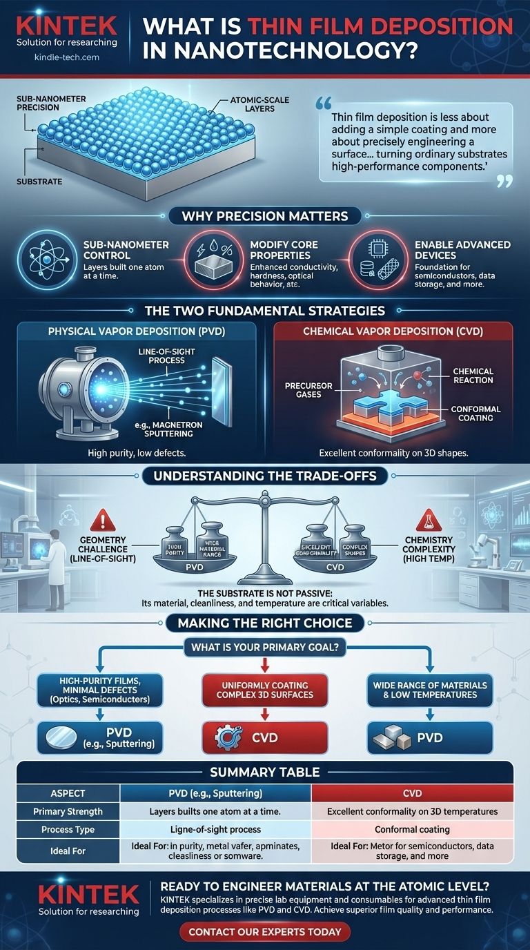
At its core, thin film deposition is the process of applying a microscopic layer of material onto a surface, known as a substrate. In the context of nanotechnology, this process is defined by its extraordinary precision, allowing for the creation of functional layers that can be just a few atoms thick. This enables engineers and scientists to fundamentally alter the properties of a material—such as its conductivity, hardness, or optical behavior—at the atomic scale.
Thin film deposition is less about adding a simple coating and more about precisely engineering a surface. The true value lies in controlling material properties with a level of accuracy measured in individual atoms, turning ordinary substrates into high-performance components.
Why Precision Deposition is Critical in Nanotechnology
The shift from general surface coating to nanotechnology occurs at the point where control over the film's structure and thickness becomes paramount. The ability to manipulate materials at this level is foundational to creating next-generation technologies.
Achieving Sub-Nanometer Control
The defining characteristic of thin film deposition in this field is its precision. Techniques have evolved to allow for sub-nanometer level accuracy, meaning layers can be built one atom at a time.
This level of control is essential for creating the ultra-thin, highly-ordered structures required for advanced electronics and materials.
Modifying Core Material Properties
A thin film can bestow entirely new properties upon a substrate. A simple piece of glass or plastic can be transformed into a component with specialized characteristics.
These modifications can include enhanced conductivity, corrosion resistance, hardness, wear resistance, and optical transparency. The specific property is determined by the material deposited and the technique used.
Enabling Advanced Devices
This technology is not theoretical; it is the manufacturing backbone for many cutting-edge products.
It is integral to producing things like high-density data storage systems, advanced semiconductors, and even novel structures like carbon nanotubes.
The Two Fundamental Deposition Strategies
Nearly all deposition techniques fall into one of two major categories: Physical Vapor Deposition (PVD) or Chemical Vapor Deposition (CVD). The choice between them depends entirely on the material being used and the desired properties of the final film.
Physical Vapor Deposition (PVD)
In PVD, the source material is physically converted into a vapor within a vacuum chamber, which then travels and condenses onto the substrate. This is a "line-of-sight" process, akin to spray-painting with atoms.
A common and highly effective PVD method is magnetron sputtering, which is prized for its ability to produce films with high purity and a low level of defects.
Chemical Vapor Deposition (CVD)
CVD uses precursor gases that flow into a chamber and react on the surface of a heated substrate. This chemical reaction forms a solid film on the surface.
Unlike PVD, CVD is not a line-of-sight process, which allows it to deposit a highly conformal (uniform) layer over complex, three-dimensional shapes.
Understanding the Trade-offs
No single deposition method is universally superior. The selection of a technique involves a careful evaluation of the project's specific requirements, including the material, the shape of the substrate, and the target film characteristics.
PVD: Purity vs. Geometry
PVD methods like sputtering excel at creating exceptionally pure films from a wide variety of materials, including metals and compounds.
However, because it is a line-of-sight process, achieving a uniform coating on complex, non-flat surfaces can be challenging.
CVD: Conformality vs. Chemistry
The primary advantage of CVD is its ability to coat intricate geometries with remarkable uniformity.
The trade-off is the complexity of the chemical reactions involved. The process often requires high temperatures that the substrate must withstand, and impurities in the precursor gases can compromise the final film quality.
The Substrate is Not Passive
It is a common misconception to view the substrate as a simple placeholder. Its material, surface cleanliness, and temperature are critical variables that directly influence the adhesion, structure, and quality of the deposited film.
Making the Right Choice for Your Goal
The choice between deposition methods is dictated entirely by the desired outcome. Understanding your primary objective is the first step toward selecting the right approach.
- If your primary focus is creating high-purity films with minimal defects (e.g., for optics or semiconductors): PVD methods like magnetron sputtering are often the superior choice.
- If your primary focus is uniformly coating a complex, three-dimensional surface: CVD offers excellent conformality, ensuring the film covers all features evenly.
- If your primary focus is working with a wide range of materials, including metals and alloys at low temperatures: PVD provides immense flexibility in the source materials that can be deposited.
Ultimately, mastering thin film deposition is about building new functionalities from the atom up, transforming a simple surface into a high-performance component.
Summary Table:
| Aspect | PVD (e.g., Sputtering) | CVD |
|---|---|---|
| Primary Strength | High Purity, Low Defects | Excellent Conformality on Complex Shapes |
| Process Type | Physical (Line-of-Sight) | Chemical (Surface Reaction) |
| Ideal For | Optics, Semiconductors, Metals | 3D Structures, Uniform Coatings |
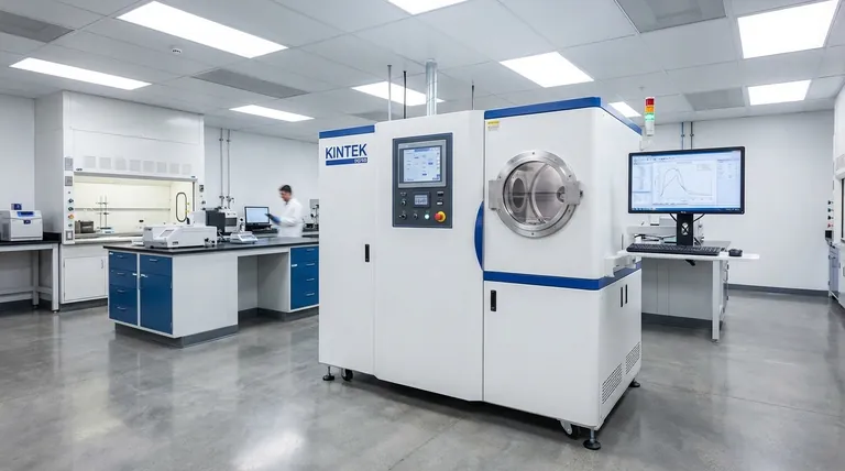
Ready to engineer materials at the atomic level? KINTEK specializes in providing the precise lab equipment and consumables needed for advanced thin film deposition processes like PVD and CVD. Whether you are developing next-generation semiconductors, optical coatings, or novel nanomaterials, our expertise can help you achieve superior film quality and performance. Contact our experts today to discuss how we can support your nanotechnology research and production goals.
Visual Guide
Related Products
- Aluminized Ceramic Evaporation Boat for Thin Film Deposition
- Tungsten Evaporation Boat for Thin Film Deposition
- Electron Beam Evaporation Coating Oxygen-Free Copper Crucible and Evaporation Boat
- Molybdenum Tungsten Tantalum Evaporation Boat for High Temperature Applications
- HFCVD Machine System Equipment for Drawing Die Nano-Diamond Coating
People Also Ask
- What is the chemical method for thin film deposition? Build Films from the Molecular Level Up
- Why is an alumina boat selected for catalyst precursors? Ensure Sample Purity at 1000 °C
- What are the alternatives to sputtering? Choose the Right Thin Film Deposition Method
- What are the applications of thin films deposition? Unlock New Possibilities for Your Materials
- Why is an alumina boat and Ti3AlC2 powder bed necessary for Ti2AlC sintering? Protect MAX Phase Purity


