Plasma-Enhanced Chemical Vapor Deposition (PECVD) is primarily utilized to deposit a wide range of silicon-based thin films, specialized carbon coatings, and various metals. The most frequently deposited materials include Silicon Nitride, Silicon Oxide, Silicon Dioxide, Silicon OxyNitride, Amorphous Silicon, Poly Silicon, and Diamond-Like Carbon (DLC).
Core Takeaway PECVD is defined by its versatility, allowing for the low-temperature deposition of critical dielectric and semiconductor materials. It is the method of choice for creating high-quality insulating layers and conductive films on substrates that cannot withstand the high thermal loads of traditional deposition processes.
Categorizing PECVD Materials
To understand the capabilities of PECVD, it is helpful to categorize the materials by their function within an electronic or engineering device.
Silicon-Based Dielectrics
The most common application for PECVD is the creation of insulating layers.
Silicon Oxide and Silicon Dioxide are standard materials used for electrical insulation and passivation layers in semiconductor devices.
Silicon Nitride offers excellent moisture barriers and mechanical protection, often used as a final passivation layer.
Silicon OxyNitride serves as a versatile intermediate, combining properties of both oxides and nitrides to tune the refractive index or stress of the film.
Semiconductor Films
PECVD is instrumental in depositing the active layers of electronic components.
Amorphous Silicon is widely deposited for use in solar cells, thin-film transistors (TFTs), and optical sensors.
Poly Silicon (Polycrystalline Silicon) is used for gate electrodes and interconnects, offering higher electron mobility than amorphous varieties.
Protective and Hard Coatings
Beyond electronics, PECVD is used for mechanical surface engineering.
Diamond-Like Carbon (DLC) is a critical material deposited for its extreme hardness, low friction, and wear resistance.
Metallic and Ceramic Capabilities
While silicon-based materials are the primary use case, the process is highly adaptable.
PECVD can deposit various metallic and ceramic coatings, provided appropriate precursors are available.
This includes specific metals derived from organometallic or metal coordination complexes.
Understanding the Process Constraints
While PECVD is versatile, material selection is dictated by chemical realities.
Precursor Dependency
You cannot deposit a material via PECVD unless a suitable volatile precursor exists.
The process relies on introducing gases (like silane) or volatilized liquids (organometallics) into the chamber.
If the source material cannot be turned into a stable vapor or gas that decomposes cleanly in plasma, PECVD is not a viable option.
Chemical By-Products
The formation of solid films creates volatile by-products that must be continuously removed.
The efficiency of the deposition depends on how easily these ligands are lost to the gas phase during the reaction on the wafer surface.
Making the Right Choice for Your Goal
Selecting the correct material depends entirely on the functional requirements of your thin film.
- If your primary focus is electrical insulation: Prioritize Silicon Dioxide or Silicon Nitride for robust dielectric properties and passivation.
- If your primary focus is active device fabrication: Utilize Amorphous Silicon or Poly Silicon to create the conductive pathways and active semiconductor layers.
- If your primary focus is surface durability: Choose Diamond-Like Carbon (DLC) to enhance wear resistance and hardness.
PECVD transforms volatile precursors into solid, high-performance films, bridging the gap between delicate substrates and robust material requirements.
Summary Table:
| Material Category | Common Thin Films | Primary Applications |
|---|---|---|
| Silicon-Based Dielectrics | Silicon Oxide, Silicon Dioxide, Silicon Nitride | Electrical insulation, passivation layers, moisture barriers |
| Semiconductor Films | Amorphous Silicon, Poly Silicon | Solar cells, TFTs, optical sensors, gate electrodes |
| Hard Coatings | Diamond-Like Carbon (DLC) | Wear resistance, low friction, surface durability |
| Specialized Films | Silicon OxyNitride, Metallic/Ceramic coatings | Refractive index tuning, interconnects, surface engineering |
Elevate Your Thin Film Deposition with KINTEK
Ready to achieve superior film quality and precision in your research? KINTEK specializes in advanced laboratory solutions, including high-performance CVD and PECVD systems tailored for semiconductor and materials science.
Our extensive portfolio supports your entire workflow—from high-temperature furnaces and crushing systems to battery research tools and high-pressure reactors. Whether you are depositing silicon-based dielectrics or specialized DLC coatings, KINTEK provides the reliability and expertise your lab demands.
Contact us today to find the perfect PECVD solution for your application!
Related Products
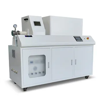
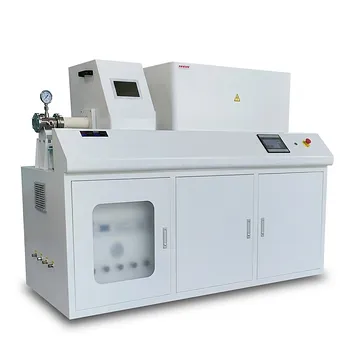
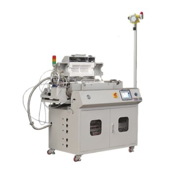
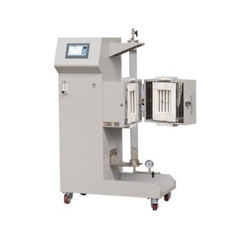
- Inclined Rotary Plasma Enhanced Chemical Vapor Deposition PECVD Equipment Tube Furnace Machine
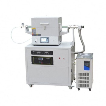
- Chemical Vapor Deposition CVD Equipment System Chamber Slide PECVD Tube Furnace with Liquid Gasifier PECVD Machine
- Inclined Rotary Plasma Enhanced Chemical Vapor Deposition PECVD Equipment Tube Furnace Machine
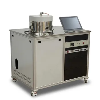
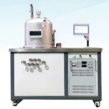
- RF PECVD System Radio Frequency Plasma-Enhanced Chemical Vapor Deposition RF PECVD
- Multi Heating Zones CVD Tube Furnace Machine Chemical Vapor Deposition Chamber System Equipment
People Also Ask
- What are the core advantages of PE-CVD in OLED encapsulation? Protect Sensitive Layers with Low-Temp Film Deposition
- How does PECVD equipment facilitate the directional growth of carbon nanotubes? Achieve Precision Vertical Alignment
- What is plasma enhanced chemical vapor deposition PECVD equipment? A Guide to Low-Temperature Thin Film Deposition
- How does plasma enhanced chemical vapor deposition work? Enable Low-Temperature Thin Film Deposition
- What is plasma enhanced chemical vapour deposition PECVD used for? Enable Low-Temp Thin Films for Electronics & Solar
