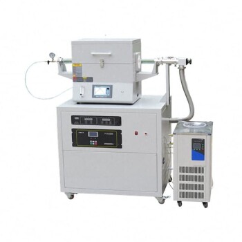
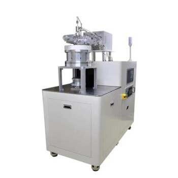
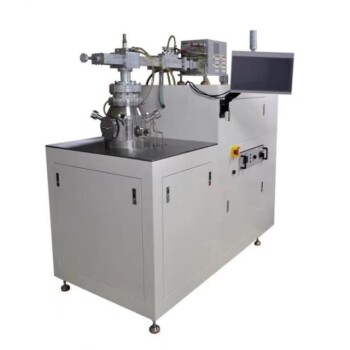
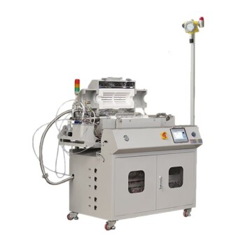
PECVD systems operate at low pressure and low temperature to achieve high-quality film deposition on sensitive substrates without causing thermal damage. By maintaining a low-pressure environment, the system reduces particle scattering to ensure uniform film thickness. Simultaneously, low-temperature processing protects the substrate from warping or chemical degradation by substituting high heat with plasma energy to drive the necessary chemical reactions.
The Core Takeaway In Plasma Enhanced Chemical Vapor Deposition (PECVD), energy is the currency. By supplying energy through an electrically driven plasma rather than thermal heat, PECVD decouples the deposition process from high temperatures, allowing for precise coating on delicate electronics that would otherwise be destroyed by traditional CVD methods.
The Physics of Low Pressure
Increasing the Mean Free Path
Operating at low pressure (typically below 0.1 Torr to 1 Torr) significantly reduces the density of gas particles within the chamber. This increases the "mean free path," which is the average distance a particle travels before colliding with another.
Improving Film Uniformity
Because particles collide less frequently in the gas phase, the deposition process becomes more predictable and controlled. This reduction in scattering promotes a highly uniform film layer across the entire surface of the substrate.
Stabilizing the Plasma Discharge
Low pressure is essential for maintaining a stable glow discharge. It creates the optimal environment for the plasma species to exist and react, ensuring the deposition process remains consistent throughout the cycle.
Minimizing Unwanted Reactions
High pressure can lead to premature chemical reactions in the vapor phase before the gas reaches the substrate (creating dust rather than a film). Low pressure minimizes these unwanted vapor-phase reactions, ensuring the material forms correctly on the target surface.
The Strategic Advantage of Low Temperature
Substituting Heat with Plasma Energy
Traditional CVD relies on heat to break chemical bonds, but PECVD uses Radio Frequency (RF) induced glow discharge (typically 100–300 eV). This discharge generates high-energy free electrons that collide with reactant gases to dissociate them.
Reducing Thermal Requirements
Because the plasma provides a significant portion of the energy required for the chemical reaction, the thermal load on the system is drastically reduced. This allows the process to occur at temperatures ranging from room temperature up to roughly 400°C, rather than the much higher temperatures required by thermal CVD.
Protecting Sensitive Substrates
Low-temperature operation is critical for substrates that cannot withstand high heat, such as glass used in active matrix LCD displays or fully manufactured electronic components. It allows for the deposition of layers like silicon nitride or silicon oxide without melting or warping the base material.
Preventing Chemical Interdiffusion
High temperatures often cause materials to diffuse into one another, blurring the lines between layers. Low-temperature PECVD minimizes this interdiffusion and prevents unwanted chemical reactions between the new film layer and the underlying substrate material.
Understanding the Trade-offs
Vacuum System Complexity
To achieve the benefits of low pressure, PECVD systems require robust vacuum infrastructure. Maintaining pressures below 0.1 Torr demands sophisticated pumping systems and vacuum seals, adding to the equipment's complexity and maintenance requirements compared to atmospheric processes.
Energy Source Management
While thermal energy is reduced, it is replaced by RF energy management. The system must carefully balance the RF power to generate sufficient plasma density without damaging the film or the substrate with excessive ion bombardment.
Making the Right Choice for Your Goal
When evaluating deposition methods for your specific application, consider the following operational priorities:
- If your primary focus is Substrate Integrity: PECVD is the ideal choice for coating temperature-sensitive components (like VLSI circuits or TFTs) to prevent thermal warping and interlayer diffusion.
- If your primary focus is Film Uniformity: The low-pressure environment of PECVD provides superior control over step coverage and thickness consistency compared to atmospheric processes.
- If your primary focus is Manufacturing Throughput: PECVD offers higher deposition rates than Atomic Layer Deposition (ALD), making it more suitable for high-volume production where speed is a factor.
By leveraging plasma physics to lower temperature and pressure requirements, PECVD bridges the gap between high-speed production and the delicate nature of modern microelectronics.
Summary Table:
| Feature | Benefit of Low Pressure | Benefit of Low Temperature |
|---|---|---|
| Substrate Safety | Prevents dust/particle contamination | Avoids warping, melting, or degradation |
| Film Quality | Ensures uniform thickness and coverage | Minimizes unwanted chemical interdiffusion |
| Process Control | Increases mean free path for particles | Decouples energy source from thermal heat |
| Ideal For | High-precision microelectronics | Temperature-sensitive glass and polymers |
Elevate Your Thin-Film Research with KINTEK
Precise control over pressure and temperature is non-negotiable for high-quality film deposition. KINTEK specializes in advanced laboratory equipment, providing state-of-the-art PECVD, CVD, and vacuum furnace systems designed specifically for the rigorous demands of modern microelectronics and material science.
Whether you are developing active-matrix LCDs, VLSI circuits, or next-generation batteries, our team of experts is ready to equip your lab with high-performance crushing systems, hydraulic presses, and high-temperature reactors tailored to your research goals.
Ready to optimize your deposition process? Contact KINTEK today to discover how our comprehensive portfolio of laboratory solutions can enhance your production efficiency and substrate integrity.
Related Products
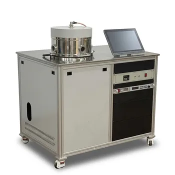
- RF PECVD System Radio Frequency Plasma-Enhanced Chemical Vapor Deposition RF PECVD
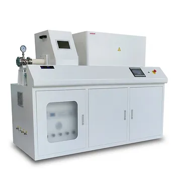
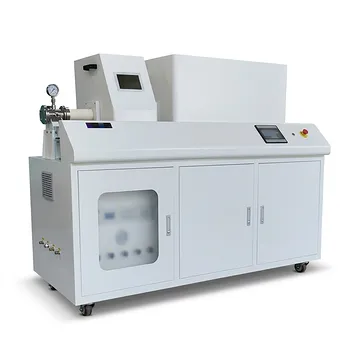
- Chemical Vapor Deposition CVD Equipment System Chamber Slide PECVD Tube Furnace with Liquid Gasifier PECVD Machine
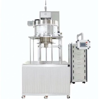
- Inclined Rotary Plasma Enhanced Chemical Vapor Deposition PECVD Equipment Tube Furnace Machine
- Inclined Rotary Plasma Enhanced Chemical Vapor Deposition PECVD Equipment Tube Furnace Machine
- 915MHz MPCVD Diamond Machine Microwave Plasma Chemical Vapor Deposition System Reactor
People Also Ask
- What is plasma enhanced chemical vapour deposition process? Unlock Low-Temperature, High-Quality Thin Films
- How does plasma enhance CVD? Unlock Low-Temperature, High-Quality Film Deposition
- What is plasma enhanced chemical vapour deposition PECVD used for? Enable Low-Temp Thin Films for Electronics & Solar
- What is plasma enhanced chemical Vapour deposition process used for fabrication of? A Guide to Low-Temperature Thin Films
- How does Radio Frequency Enhanced Plasma Chemical Vapour Deposition (RF-PECVD) work? Learn the Core Principles

