In Plasma Enhanced Chemical Vapor Deposition (PECVD), optimizing pole plate spacing and reaction chamber size is a critical exercise in balancing film quality against production efficiency. Pole plate spacing primarily determines the starting voltage and plasma potential, directly influencing substrate damage and deposition uniformity. Meanwhile, the size of the reaction chamber dictates system productivity but presents challenges for maintaining consistent film thickness across the batch.
Success in PECVD configuration requires a precise trade-off: widening plate spacing protects the substrate but risks uneven deposition near the edges, while enlarging the chamber boosts throughput at the cost of thickness uniformity.
Optimizing Pole Plate Spacing
Regulating Plasma Potential
The primary objective of adjusting plate spacing is to achieve a low starting voltage. Lowering this voltage reduces the overall plasma potential during the deposition process. This is essential for minimizing potential damage to the substrate caused by high-energy ion bombardment.
The Impact of Increased Spacing
Widening the gap between electrodes is generally effective for lessening substrate damage. By optimizing this distance, you protect the sensitive features of the device from the aggressive nature of the plasma discharge.
The Risk of Excessive Spacing
However, spacing cannot be increased indefinitely without consequence. If the gap becomes too large, it aggravates the electric field's edge effect. This distortion leads to poor deposition uniformity, resulting in inconsistent film properties across the wafer surface.
Sizing the Reaction Chamber
Boosting Productivity
Scaling up the reaction chamber size is the most direct method to increase productivity. A larger chamber volume allows for higher throughput, which is essential for scaling semiconductor manufacturing.
Managing Thickness Variations
The downside of a larger volume is the difficulty in maintaining consistent conditions throughout the entire space. Consequently, larger chambers often struggle with the uniformity of film thickness. As the chamber scales up, ensuring that the film grows at the same rate in all areas becomes significantly more challenging.
Understanding the Trade-offs
Uniformity vs. Substrate Integrity
You are often forced to choose between physical film uniformity and the electronic integrity of the substrate. Prioritizing a wider gap protects the device structure but requires accepting a higher risk of edge variations in the electric field.
Throughput vs. Process Control
Similarly, high-volume manufacturing demands large chambers, but this introduces process variability. Higher productivity yields are counterproductive if the thickness variation across the batch renders the final devices unusable.
Making the Right Choice for Your Goal
To optimize your PECVD process, you must align these physical parameters with your specific manufacturing priorities:
- If your primary focus is sensitive substrate protection: Increase pole plate spacing to lower the starting voltage and plasma potential, while carefully monitoring for edge effect distortions.
- If your primary focus is film uniformity: Maintain a tighter pole plate spacing to stabilize the electric field and minimize edge effects, ensuring even deposition across the wafer.
- If your primary focus is high-volume throughput: Utilize a larger reaction chamber to maximize productivity, but implement rigorous controls to mitigate potential variances in film thickness.
Precise calibration of these geometric parameters ensures the optimal balance between protecting your device and meeting production targets.
Summary Table:
| Parameter | Primary Impact | Benefits of Increase | Risks of Increase |
|---|---|---|---|
| Pole Plate Spacing | Plasma Potential & Uniformity | Lower starting voltage; reduced substrate damage | Edge effect distortions; poor deposition uniformity |
| Chamber Size | Productivity & Thickness | Higher throughput and production volume | Challenging film thickness uniformity across the batch |
Elevate Your Thin-Film Deposition Precision with KINTEK
Achieving the perfect balance between film uniformity and substrate integrity requires more than just process knowledge—it demands high-performance equipment. KINTEK specializes in advanced laboratory solutions, including state-of-the-art PECVD and CVD systems designed to give you precise control over every geometric parameter.
Whether you are scaling up semiconductor manufacturing or conducting sensitive materials research, our portfolio offers the tools you need for success:
- High-Temperature Furnaces: Precise PECVD, CVD, and MPCVD solutions.
- Material Processing: From crushing, milling, and sieving to hydraulic pellet presses.
- Lab Essentials: High-pressure reactors, autoclaves, and specialized ceramics/crucibles.
Don't let process variability hinder your productivity. Let our experts help you configure the ideal system for your specific research or production goals.
Contact KINTEK today to optimize your lab's efficiency!
Related Products
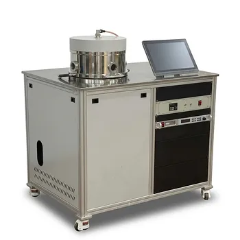
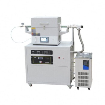
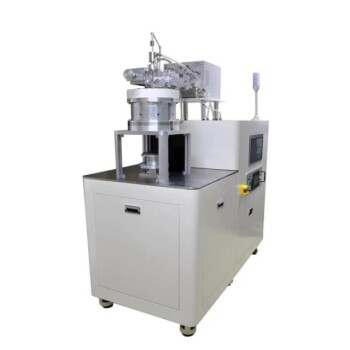
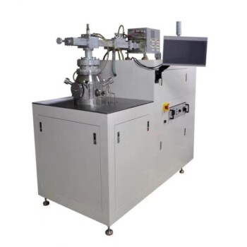
- RF PECVD System Radio Frequency Plasma-Enhanced Chemical Vapor Deposition RF PECVD
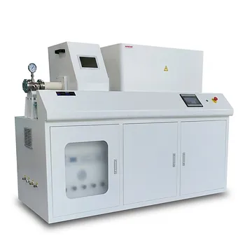
- Chemical Vapor Deposition CVD Equipment System Chamber Slide PECVD Tube Furnace with Liquid Gasifier PECVD Machine
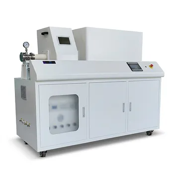
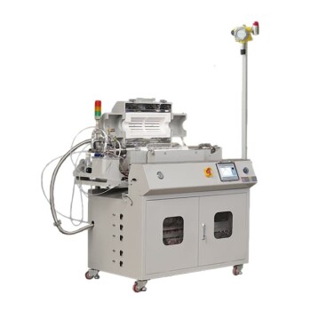
- Inclined Rotary Plasma Enhanced Chemical Vapor Deposition PECVD Equipment Tube Furnace Machine
- Inclined Rotary Plasma Enhanced Chemical Vapor Deposition PECVD Equipment Tube Furnace Machine
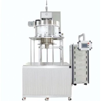
- 915MHz MPCVD Diamond Machine Microwave Plasma Chemical Vapor Deposition System Reactor
People Also Ask
- How does Radio Frequency Enhanced Plasma Chemical Vapour Deposition (RF-PECVD) work? Learn the Core Principles
- What is an example of PECVD? RF-PECVD for High-Quality Thin Film Deposition
- What is plasma enhanced chemical Vapour deposition process used for fabrication of? A Guide to Low-Temperature Thin Films
- What is plasma enhanced chemical vapour deposition process? Unlock Low-Temperature, High-Quality Thin Films
- What is plasma enhanced chemical vapour deposition PECVD used for? Enable Low-Temp Thin Films for Electronics & Solar

