The thickness of a Chemical Vapor Deposition (CVD) coating is not a single value, but a highly controllable parameter. This process is renowned for its precision, allowing for the creation of films that range from a single layer of atoms (nanometers) up to several micrometers thick, depending entirely on the specific application and process variables.
The core strength of Chemical Vapor Deposition is its precise control over film thickness. This versatility allows it to produce everything from the atomically thin layers required for modern electronics to thicker, more robust coatings for wear resistance.
What is Chemical Vapor Deposition?
The Core Process
Chemical Vapor Deposition is a manufacturing process that uses a vacuum chamber to deposit a solid material from a gaseous state onto a surface, known as a substrate.
Volatile chemical precursors are introduced into the chamber. A chemical reaction is then induced, typically by heat, causing the material to deposit onto the workpiece.
Key Characteristics
The result of this process is an exceptionally pure, dense, and uniform thin film. Because the precursor gases can flow around complex geometries, CVD is excellent for evenly coating intricate shapes.
The Factors That Determine CVD Thickness
The final thickness of a CVD coating is a direct result of several carefully managed process parameters. Full control over these variables is what makes the technology so versatile.
Process Duration
The most straightforward factor is time. The longer the substrate is exposed to the deposition process, the more material will accumulate, resulting in a thicker film.
Precursor Flow and Concentration
The rate at which the precursor chemicals are introduced into the chamber directly influences the growth rate. A higher flow rate generally leads to faster deposition and a thicker coating in a given amount of time.
Temperature and Pressure
Temperature and pressure within the vacuum chamber are critical. These conditions dictate the speed of the chemical reactions on the substrate's surface. Optimizing them is key to controlling not only thickness but also the film's quality and structure.
Understanding the "Ultra-Thin" Advantage
The references highlight CVD's ability to create "ultra-thin layers," which is one of its most significant advantages, particularly in high-tech industries.
Applications in Electronics
The production of microprocessors and electrical circuits relies on depositing atomically precise layers of conductive and insulating materials. CVD provides the exact level of control needed to build these complex, microscopic structures.
Purity at Any Scale
Whether depositing a film that is a few nanometers or several micrometers thick, CVD produces materials of exceptionally high purity. This ensures predictable and reliable performance, which is non-negotiable in fields like semiconductor manufacturing.
Common Trade-offs to Consider
While powerful, the CVD process involves balancing competing priorities to achieve the desired outcome.
Speed vs. Precision
Generally, depositing thicker films can be done at a higher rate. However, achieving a perfectly uniform, ultra-thin film with atomic-level precision often requires a slower, more meticulously controlled process.
Cost and Complexity
The equipment required for high-precision CVD is sophisticated and expensive. Gaining precise control over temperature, pressure, and gas flow for advanced applications adds to the operational complexity and cost.
Material and Substrate Compatibility
The process is fundamentally based on chemical reactions. The choice of precursor chemicals is limited to those that will react appropriately at temperatures the substrate can withstand without being damaged.
Matching Thickness to Your Application
Your final thickness requirement will determine how you approach the CVD process.
- If your primary focus is semiconductor manufacturing: You will leverage CVD for its ability to create exceptionally pure and uniform films, often just a few nanometers thick.
- If your primary focus is wear-resistant coatings (e.g., on cutting tools): You will use CVD to build up much thicker, harder layers, typically in the micrometer range, for enhanced durability.
- If your primary focus is creating optical films: You will need precise thickness control in the nanometer range to manipulate light reflectivity and transmission for lenses or sensors.
Ultimately, the thickness of a CVD coating is defined by the specific needs of your project.
Summary Table:
| Target Thickness Range | Primary Applications | Key Considerations |
|---|---|---|
| Nanometers (nm) | Semiconductors, Microelectronics, Optical Films | Requires high precision, slower deposition, focus on purity and uniformity |
| Micrometers (µm) | Wear-Resistant Coatings, Cutting Tools, Thick Protective Layers | Faster deposition possible, prioritizes durability and hardness |
| Highly Controllable | Custom applications across industries | Balance of speed, precision, cost, and substrate compatibility |
Need a CVD coating with precise thickness for your application? KINTEK specializes in lab equipment and consumables, providing solutions for semiconductor manufacturing, wear-resistant coatings, and optical films. Our expertise ensures you get the exact film thickness, purity, and performance your project demands. Contact us today to discuss your specific requirements and discover how our CVD solutions can enhance your laboratory's capabilities!
Related Products
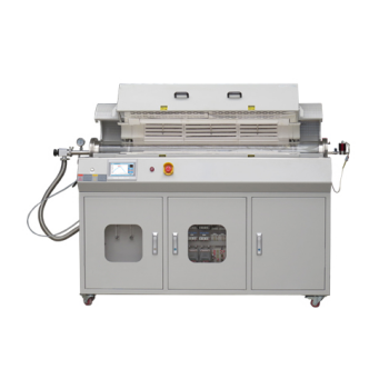
- Chemical Vapor Deposition CVD Equipment System Chamber Slide PECVD Tube Furnace with Liquid Gasifier PECVD Machine
- RF PECVD System Radio Frequency Plasma-Enhanced Chemical Vapor Deposition RF PECVD
- Vacuum Hot Press Furnace Machine for Lamination and Heating
- Laboratory CVD Boron Doped Diamond Materials
- Vacuum Hot Press Furnace Heated Vacuum Press Machine Tube Furnace
People Also Ask
- What are the examples of CVD method? Discover the Versatile Applications of Chemical Vapor Deposition
- What are the benefits of plasma enhanced CVD? Achieve High-Quality, Low-Temperature Film Deposition
- How are PECVD and CVD different? A Guide to Choosing the Right Thin-Film Deposition Process
- What is the difference between CVD and PECVD? Choose the Right Thin-Film Deposition Method
- Can plasma enhanced CVD deposit metals? Why PECVD is rarely used for metal deposition