Yes, Chemical Vapor Deposition (CVD) is a foundational chemical process used to produce some of the most advanced materials in modern technology. It works by introducing reactive gases (precursors) into a chamber, where they undergo a chemical reaction and deposit a high-purity, solid thin film onto a surface (substrate). This method is indispensable for manufacturing everything from computer chips to durable coatings for industrial tools.
CVD is not simply a coating technique; it is a method of atomic-scale engineering. By precisely controlling gas-phase chemical reactions, we can construct ultra-pure and highly uniform thin films with properties that are often impossible to achieve through conventional means.

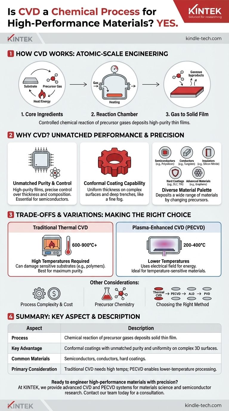
How CVD Works at a Fundamental Level
To understand why CVD is so powerful, you must first understand its core mechanism. The process is a carefully orchestrated sequence of events happening within a controlled environment.
The Core Ingredients
The process relies on three key components: a substrate, which is the material to be coated; precursors, which are volatile gases containing the atoms you wish to deposit; and energy, typically in the form of heat, to drive the chemical reaction.
The Reaction Chamber Environment
CVD is performed in a sealed vacuum chamber. This controlled environment is critical for two reasons: it prevents unwanted reactions with air (like oxidation) and it allows for precise control over the pressure and concentration of the precursor gases.
From Gas to Solid Film
Once the substrate is heated to the target temperature, the precursor gases are introduced. These gases diffuse towards the hot substrate, where they decompose and react. This chemical reaction results in the desired solid material "condensing" or depositing onto the substrate, building up a thin film one layer of atoms at a time.
The Creation of Byproducts
As the name "Chemical Vapor Deposition" implies, a true chemical reaction occurs. This means that in addition to the solid film, gaseous byproducts are also created. These waste products are continuously removed from the chamber by the vacuum system.
Why CVD is Essential for High-Performance Materials
The unique nature of the CVD process is directly responsible for the superior qualities of the films it produces. It's chosen when performance, purity, and precision are non-negotiable.
Unmatched Purity and Control
Because the precursors are highly purified gases, the resulting films can achieve exceptional purity levels. This is absolutely critical in the semiconductor industry, where even a few foreign atoms can ruin a microchip. The process allows for precise control over the film's thickness and composition.
Conformal Coating Capability
One of CVD's most significant advantages is its ability to create conformal coatings. This means the film deposits with a perfectly uniform thickness over complex, three-dimensional surfaces and deep trenches. Think of it not as spray painting a surface from one angle, but as a fog that settles evenly over every feature of an intricate landscape.
A Diverse Material Palette
CVD is not limited to a single material. By changing the precursor gases, an incredibly wide range of materials can be deposited, including:
- Semiconductors: Polysilicon and silicon dioxide for microchips.
- Conductors: Tungsten and copper for wiring within chips.
- Insulators: Silicon nitride and silicon oxynitride to electrically isolate components.
- Hard Coatings: Diamond-like carbon (DLC) and titanium nitride (TiN) for wear-resistant tools.
- Advanced Materials: Graphene and other 2D materials for next-generation electronics.
Understanding the Trade-offs and Variations
While powerful, CVD is not a universal solution. Understanding its limitations is key to using it effectively.
High Temperature Requirements
Traditional thermal CVD often requires very high temperatures (600-900°C or higher) to provide the energy needed for the chemical reactions. These temperatures can damage or melt many substrates, such as plastics or fully processed silicon wafers.
The Solution: Plasma-Enhanced CVD (PECVD)
To overcome temperature limitations, Plasma-Enhanced CVD (PECVD) was developed. In this variation, an electrical field is used to create a plasma (an ionized gas). The energetic plasma provides the energy to break down the precursor gases at much lower temperatures (typically 200-400°C), making it compatible with more sensitive materials.
Process Complexity and Cost
CVD reactors are complex and expensive pieces of equipment. They require sophisticated control over high-vacuum systems, gas flows, temperature, and power supplies. The process can also be slower than other deposition methods like Physical Vapor Deposition (PVD).
The Challenge of Precursor Chemistry
The success of a CVD process hinges on the precursor chemicals. An ideal precursor must be volatile enough to be transported as a gas, stable enough not to decompose during delivery, and reactive enough to deposit a pure film at the desired temperature without leaving behind contaminants. Developing and sourcing these chemicals can be a significant challenge.
Making the Right Choice for Your Goal
Selecting the correct deposition method depends entirely on the material, the substrate, and the desired outcome.
- If your primary focus is maximum film purity and crystallinity: Traditional, high-temperature thermal CVD is often the gold standard, provided your substrate can tolerate the heat.
- If you are working with temperature-sensitive substrates like polymers or processed electronics: Plasma-Enhanced CVD (PECVD) is the necessary choice to enable deposition without causing thermal damage.
- If you need absolute, atom-by-atom control for coating extremely complex 3D nanostructures: Atomic Layer Deposition (ALD), a highly controlled subtype of CVD, is the superior technique.
- If cost and deposition speed are more critical than ultimate film perfection for a simple coating: Physical Vapor Deposition (PVD) may be a more suitable alternative to investigate.
By understanding these core principles, you can select the precise technique needed to engineer materials from the atom up for your specific application.
Summary Table:
| Key Aspect | Description |
|---|---|
| Process | Chemical reaction of precursor gases deposits a solid thin film on a substrate. |
| Key Advantage | Conformal coatings with unmatched purity and uniformity on complex 3D surfaces. |
| Common Materials | Semiconductors (e.g., polysilicon), conductors (e.g., tungsten), hard coatings (e.g., TiN, DLC). |
| Primary Consideration | Traditional CVD requires high temperatures; PECVD enables lower-temperature processing. |
Ready to engineer high-performance materials with precision?
At KINTEK, we specialize in providing advanced lab equipment, including CVD and PECVD systems, to meet the demanding needs of materials science and semiconductor research. Our solutions empower you to create ultra-pure, uniform thin films for applications from microchips to wear-resistant coatings.
Let's discuss how our expertise can accelerate your R&D. Contact our team today for a consultation tailored to your laboratory's specific challenges.
Visual Guide
Related Products
- Chemical Vapor Deposition CVD Equipment System Chamber Slide PECVD Tube Furnace with Liquid Gasifier PECVD Machine
- Customer Made Versatile CVD Tube Furnace Chemical Vapor Deposition Chamber System Equipment
- HFCVD Machine System Equipment for Drawing Die Nano-Diamond Coating
- Split Chamber CVD Tube Furnace with Vacuum Station Chemical Vapor Deposition System Equipment Machine
- Multi Heating Zones CVD Tube Furnace Machine Chemical Vapor Deposition Chamber System Equipment
People Also Ask
- What types of substrates are used in CVD to facilitate graphene films? Optimize Graphene Growth with the Right Catalyst
- How are carbon nanotubes grown? Master Scalable Production with Chemical Vapor Deposition
- What are the advantages of chemical vapor deposition? Achieve Superior Thin Films for Your Lab
- How expensive is chemical vapor deposition? Understanding the True Cost of High-Performance Coating
- What are the processes of vapor phase deposition? Understand CVD vs. PVD for Superior Thin Films


