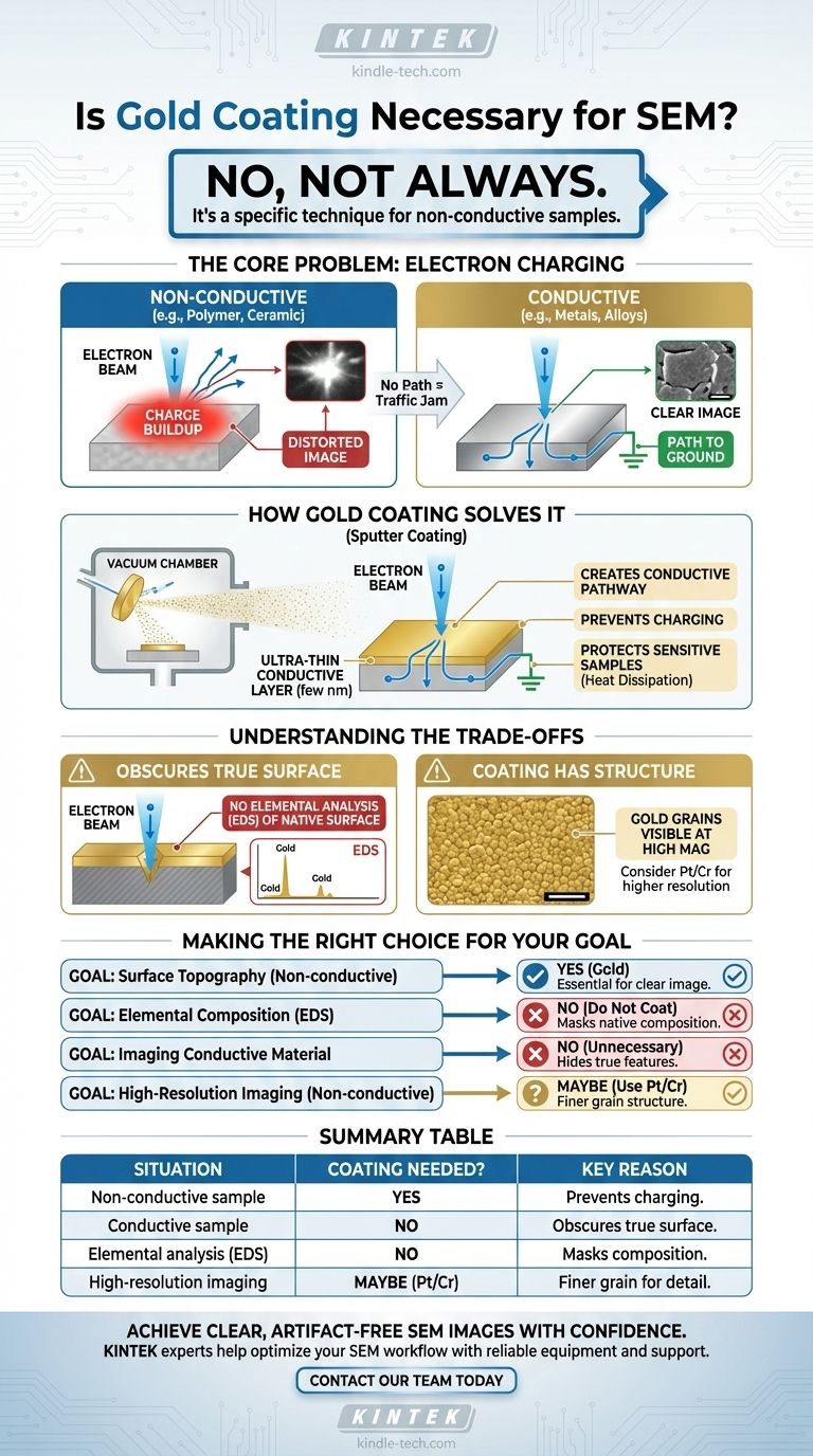
No, gold coating is not always necessary for SEM. It is a specific sample preparation technique used to enable or improve the imaging of materials that are naturally non-conductive or sensitive to the electron beam. For samples that are already electrically conductive, such as most metals and alloys, coating is unnecessary and will obscure the true surface.
The core challenge in SEM is managing the flow of electrons. Coating a non-conductive sample with a thin layer of gold creates a path for electrons to travel away from the surface, preventing a "traffic jam" that would otherwise distort the image.

The Core Problem: Electron Charging
What Happens with Non-Conductive Samples?
A Scanning Electron Microscope (SEM) works by bombarding a sample with a focused beam of electrons. To create a stable image, these electrons must have a path to ground.
Conductive materials, like metals, naturally provide this path. Non-conductive materials, such as polymers, ceramics, or biological tissue, do not.
The Buildup of Charge
Without a conductive path, electrons from the beam accumulate on the surface of the sample. This phenomenon is known as electron charging.
This buildup of negative charge repels the incoming electron beam, deflecting it unpredictably and severely degrading the resulting image.
Visual Signs of Charging
Charging artifacts are easy to spot in an SEM image. They often appear as excessively bright, distorted areas, image drift, or sharp lines and bands that obscure the actual features of your sample.
How Gold Coating Solves the Problem
Creating a Conductive Pathway
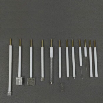
The solution to charging is to apply an ultra-thin, electrically conductive layer to the sample's surface through a process called sputter coating.
This metallic layer, often gold, is only a few nanometers thick. It conforms to the sample's topography and connects it to the grounded SEM stage, giving the excess electrons an escape route.
Why Gold is a Common Choice
Gold is widely used because it is an efficient material to sputter, causes minimal heating of the sample, and has properties that produce a good signal for imaging.
It is an excellent general-purpose coating, especially for routine imaging at low to medium magnifications.
Protecting Sensitive Samples
Sputter coating also serves a secondary purpose: it helps protect delicate, beam-sensitive samples. The conductive layer helps dissipate the energy and heat from the electron beam, reducing potential damage to the underlying structure.
Understanding the Trade-offs
You Are No Longer Imaging the True Surface
This is the most critical trade-off. Once you coat a sample, the electron beam primarily interacts with the coating, not the original material.
This means you lose the ability to perform accurate elemental analysis (like EDS) on the native surface, as the detector will mostly see the gold you deposited.
The Coating Has Its Own Structure
Gold coatings have a granular structure. At very high magnifications, you may begin to see the texture of the gold grains rather than the finest features of your sample.
For this reason, materials with a finer grain structure, like platinum or chromium, are often preferred for very high-resolution applications.
The Process Requires Optimization
Sputter coating is not a one-size-fits-all process. The operator must determine the ideal coating thickness and parameters. Too thin a coat won't prevent charging, while too thick a coat will obscure surface details.
Making the Right Choice for Your Goal
Ultimately, the decision to coat your sample depends entirely on your material and your analytical goal.
- If your primary focus is the surface topography of a non-conductive sample (e.g., polymer fracture, ceramic grain): Gold coating is likely essential to get a clear, stable image.
- If your primary focus is the elemental composition of the surface (e.g., identifying a contaminant): Do not coat the sample, as this will prevent accurate analysis of the original material.
- If your primary focus is imaging a conductive material (e.g., a metal alloy): Coating is completely unnecessary and will only hide the features you want to see.
- If your primary focus is very high-resolution imaging of a non-conductive sample: Consider a finer-grained coating material, such as platinum or chromium, instead of gold.
Understanding when and why to use a coating is fundamental to achieving meaningful results with an SEM.
Summary Table:
| Situation | Coating Needed? | Key Reason |
|---|---|---|
| Non-conductive sample (e.g., polymer, ceramic) | Yes | Prevents electron charging for clear imaging |
| Conductive sample (e.g., metal alloy) | No | Coating obscures the true surface |
| Elemental analysis (e.g., EDS) | No | Coating masks the sample's native composition |
| High-resolution imaging | Maybe (use Pt/Cr) | Finer-grained coatings preserve detail |
Achieve clear, artifact-free SEM images with confidence.
Choosing the right sample preparation technique is critical for accurate results. Whether your project involves delicate polymers, advanced ceramics, or complex alloys, KINTEK's expertise in lab equipment and consumables ensures you have the right tools and knowledge.
Let our specialists help you optimize your SEM workflow. We provide the reliable equipment and expert support to handle all your laboratory needs, from routine imaging to advanced material analysis.
Contact our team today to discuss your specific application and ensure optimal SEM performance.
Visual Guide
Related Products
- Custom CVD Diamond Coating for Lab Applications
- Electrolytic Electrochemical Cell for Coating Evaluation
- Platinum Sheet Electrode for Laboratory and Industrial Applications
- Metallographic Specimen Mounting Machine for Laboratory Materials and Analysis
- H-Type Double-Layer Optical Electrolytic Electrochemical Cell with Water Bath
People Also Ask
- Is diamond coating permanent? The Truth About Its Long-Lasting Durability
- What is diamond coating film? A Thin Layer of Diamond for Extreme Performance
- What is CVD diamond coating? Grow a Super-Hard, High-Performance Diamond Layer
- Is diamond coating worth it? Maximize Component Life and Performance
- What are the three types of coating? A Guide to Architectural, Industrial, and Special Purpose