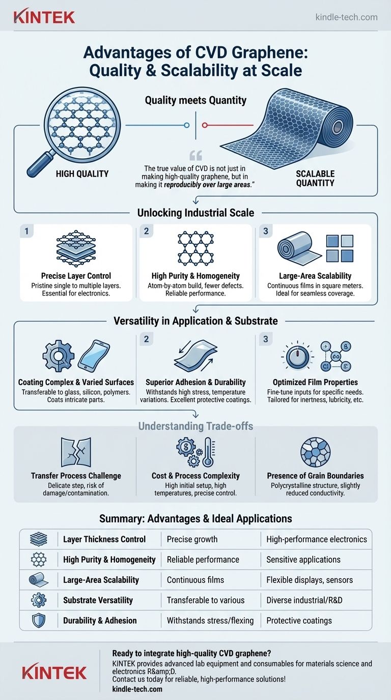
The primary advantage of CVD graphene is its unique combination of quality and scalability. Chemical Vapor Deposition (CVD) is considered a premier method for producing graphene because it yields exceptionally high-purity, large-area films with precise control over the number of layers. This makes it uniquely suited for industrial and high-performance applications where uniformity and quality are paramount.
The true value of CVD is not just in making high-quality graphene, but in making it reproducibly over large areas. This scalability is what unlocks its potential for demanding applications in electronics and advanced materials, moving it from a lab curiosity to a viable industrial material.
Unlocking Industrial Scale: Quality Meets Quantity
The challenge with graphene has always been translating its remarkable properties into real-world products. The CVD process directly addresses the primary obstacles of quality control and production volume that limit other methods.
Unprecedented Control Over Layer Thickness
CVD allows for the precise growth of graphene films, from a pristine single atomic layer to a specific number of multiple layers. This control is critical because the electronic and optical properties of graphene are highly dependent on its thickness. For applications like transparent electrodes or advanced transistors, a uniform, single layer is often essential.
High Purity and Homogeneity
The process yields graphene with high purity and structural uniformity. Unlike methods that exfoliate graphite, CVD builds the graphene sheet atom by atom from a gaseous precursor. This results in a continuous film with far fewer defects, contaminants, or unwanted chemical residues, ensuring predictable and reliable performance.
The Ability to Produce Large-Area Films
Perhaps the most significant advantage is scalability. CVD can produce continuous graphene sheets measured in square meters. This stands in stark contrast to methods that produce tiny, disconnected flakes, making CVD the only viable path for applications requiring seamless coverage, such as flexible displays, sensors, and protective coatings.
Versatility in Application and Substrate
CVD graphene is not just high-quality; it is also adaptable. The process enables its integration with a wide variety of materials and complex geometries.
Coating Complex and Varied Surfaces
While typically grown on a metal catalyst like copper, the resulting graphene film can be transferred to virtually any substrate, including glass, silicon wafers, and flexible polymers. The CVD process itself is capable of coating intricate and non-flat surfaces, ensuring uniform coverage even on complex parts.
Superior Adhesion and Durability
CVD creates a durable, well-bonded coating that remains intact even in high-stress environments. The film can withstand extreme temperature variations and even flex or bend with the substrate without delaminating. This robustness is critical for protective coatings against corrosion or wear and for the development of durable flexible electronics.
Optimized Film Properties
The process inputs, such as the precursor gas, can be fine-tuned to optimize the final film's characteristics. This allows for the creation of graphene with enhanced properties tailored to a specific need, such as chemical inertness, high lubricity, or corrosion resistance.
Understanding the Trade-offs
No method is without its challenges. An objective assessment of CVD requires understanding its inherent complexities and limitations.
The Transfer Process Challenge
The most significant hurdle for CVD graphene is the transfer step. After being grown on a metal foil, the graphene must be carefully moved to the final target substrate. This delicate process can introduce wrinkles, tears, and contamination, potentially compromising the pristine quality of the as-grown film and impacting device yield.
Cost and Process Complexity
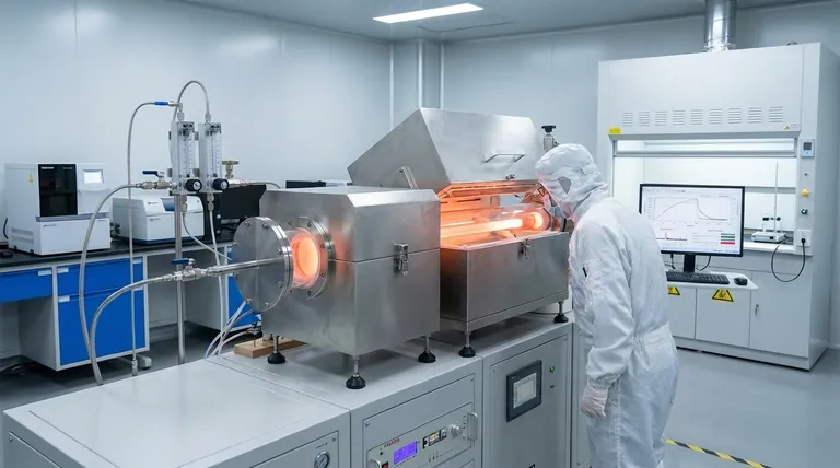
While considered cost-effective for high-end applications, the initial equipment setup for CVD is significant. It requires high-vacuum chambers, high temperatures (often around 1000°C), and precise mass-flow controllers. This complexity and cost make it less suitable for applications where bulk quantity is more important than perfect film quality.
The Presence of Grain Boundaries
CVD graphene is polycrystalline, meaning it is composed of many smaller single-crystal domains that are stitched together. The "seams" between these domains are known as grain boundaries, which can scatter electrons and slightly reduce the material's overall conductivity and mechanical strength compared to a theoretical, perfect single crystal.
Making the Right Choice for Your Application
Selecting a graphene production method depends entirely on your end goal. The trade-offs between quality, cost, and form factor are central to this decision.
- If your primary focus is high-performance electronics (e.g., transistors, transparent electrodes): CVD is the superior choice due to its ability to produce large, uniform, single-layer films with high purity.
- If your primary focus is bulk composites or conductive inks (e.g., strengthening polymers, battery additives): Other methods like liquid-phase exfoliation, which produce graphene nanoplatelets in large quantities, are likely more cost-effective and practical.
- If your primary focus is advanced protective coatings (e.g., anti-corrosion, anti-wear): CVD is a leading candidate because of its excellent conformity, substrate adhesion, and impermeability.
Ultimately, choosing CVD is a strategic decision to prioritize film quality and uniformity at an industrial scale.
Summary Table:
| Advantage | Key Benefit | Ideal For |
|---|---|---|
| Layer Thickness Control | Precise growth from single to multiple atomic layers | High-performance electronics, transparent electrodes |
| High Purity & Homogeneity | Fewer defects, contaminants, and residues | Reliable, predictable performance in sensitive applications |
| Large-Area Scalability | Continuous films measured in square meters | Flexible displays, sensors, industrial coatings |
| Substrate Versatility | Transferable to glass, silicon, polymers, and complex geometries | Diverse industrial and R&D applications |
| Durability & Adhesion | Withstands stress, temperature variations, and flexing | Robust protective coatings and flexible electronics |
Ready to integrate high-quality CVD graphene into your next project?
KINTEK specializes in providing advanced lab equipment and consumables tailored to materials science and electronics R&D. Whether you're developing next-generation sensors, flexible electronics, or protective coatings, our expertise ensures you have the right tools for precision and scalability. Contact us today to discuss how we can support your innovation with reliable, high-performance solutions!
Visual Guide
Related Products
- Laboratory CVD Boron Doped Diamond Materials
- CVD Diamond Wire Drawing Die Blanks for Precision Applications
- CVD Diamond for Thermal Management Applications
- CVD Diamond Dressing Tools for Precision Applications
- Custom CVD Diamond Coating for Lab Applications
People Also Ask
- Are CVD diamonds synthetic? Discover the Truth About Lab-Grown Diamonds
- What materials are CVD deposition? From Semiconductors to Super-Hard Coatings
- What are the advantages of BDD electrodes? Maximize Wastewater Treatment Efficiency and Durability
- What is the purpose of performing anodic polarization on BDD electrodes? Ensure Accurate & Reproducible Research Results
- What is the demand of CVD diamonds? Driven by Ethics, Purity, and Affordability


