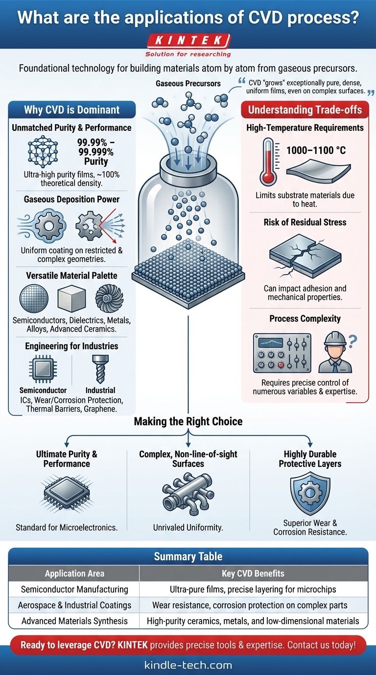
At its core, Chemical Vapor Deposition (CVD) is a foundational technology for building materials atom by atom. Its primary applications are in the semiconductor industry for creating the ultra-thin films on silicon wafers that power our electronics, in aerospace and manufacturing for applying durable protective coatings, and in materials science for synthesizing advanced, high-purity materials.
The true value of CVD lies in its unique ability to use gaseous precursors to "grow" exceptionally pure, dense, and uniform films, even on the most complex and irregular surfaces where other methods fail.
Why CVD is a Dominant Deposition Technique
Chemical Vapor Deposition is not just one process but a versatile platform. Its wide adoption stems from a few fundamental principles that give it a significant advantage for specific, high-performance applications.
Unmatched Purity and Performance
The process begins with highly pure precursor gases. This allows CVD to produce films with exceptionally high purity, often reaching 99.99% to 99.999%.
This purity, combined with the way atoms arrange themselves on the substrate, results in films that are incredibly dense—approaching 100% of their theoretical density. This eliminates porosity and creates high-performance layers.
The Power of Gaseous Deposition
Unlike line-of-sight processes like sputtering, CVD uses gases that flow and conform to any shape. This is its most significant mechanical advantage.
This allows CVD to deposit a perfectly uniform coating on restricted-access surfaces, internal channels, and other complex geometries that would be impossible to coat otherwise.
A Broad and Versatile Material Palette
CVD is not limited to a single class of materials. The process can be adapted to deposit a vast range of elements and compounds.
This includes critical materials for industry, such as semiconductors (silicon), dielectrics (silicon dioxide, silicon nitride), metals, alloys, and advanced ceramics. This flexibility makes it invaluable across many fields.
Engineering for Specific Industries
In the semiconductor industry, CVD is used to build the intricate, layered structures of integrated circuits on silicon wafers.
In industrial applications, it's used to create coatings that provide wear resistance, corrosion protection, or thermal barriers on tools, engine components, and other critical parts. It is also essential for growing low-dimensional materials like graphene.
Understanding the Inherent Trade-offs
While powerful, CVD is not a universal solution. Its process parameters introduce specific limitations and challenges that must be carefully managed.
High-Temperature Requirements
The chemical reactions that drive CVD often require very high temperatures, frequently in the range of 1000–1100 °C.
This heat limits the types of substrate materials that can be used, as many materials would melt, warp, or degrade under such conditions.
The Risk of Residual Stress
The significant difference between the high deposition temperature and room temperature can introduce residual stress into the film and substrate as the part cools.
This stress can impact the film's adhesion and mechanical properties, requiring careful control over deposition and cooling rates to mitigate.
Process Complexity
Achieving a high-quality, uniform film requires precise control over numerous variables, including the gas mixture, flow rates, temperature, and pressure. Optimizing this process for a specific application demands significant technical expertise.
Making the Right Choice for Your Goal
Selecting a deposition process depends entirely on the required properties of the final product. CVD excels where purity, conformity, and density are non-negotiable.
- If your primary focus is ultimate material purity and performance: CVD is the standard for applications like microelectronics, where even minuscule impurities can cause device failure.
- If your primary focus is coating complex, non-line-of-sight surfaces: CVD's use of gaseous precursors gives it an unrivaled ability to create uniform films on intricate geometries.
- If your primary focus is creating highly durable protective layers: The dense, low-porosity ceramic and metallic films produced by CVD offer superior protection against wear and corrosion.
By understanding its core principles, you can leverage Chemical Vapor Deposition to engineer materials with properties that are simply unattainable by other means.
Summary Table:
| Application Area | Key CVD Benefits |
|---|---|
| Semiconductor Manufacturing | Ultra-pure films, precise layering for microchips |
| Aerospace & Industrial Coatings | Wear resistance, corrosion protection on complex parts |
| Advanced Materials Synthesis | High-purity ceramics, metals, and low-dimensional materials |
Ready to leverage CVD for your high-performance coating needs? KINTEK specializes in lab equipment and consumables, providing the precise tools and expertise needed for semiconductor research, materials science, and industrial applications. Contact us today to discuss how our solutions can enhance your deposition processes and material outcomes.
Visual Guide
Related Products
- HFCVD Machine System Equipment for Drawing Die Nano-Diamond Coating
- Custom CVD Diamond Coating for Lab Applications
- Chemical Vapor Deposition CVD Equipment System Chamber Slide PECVD Tube Furnace with Liquid Gasifier PECVD Machine
- Customer Made Versatile CVD Tube Furnace Chemical Vapor Deposition Chamber System Equipment
- Multi Heating Zones CVD Tube Furnace Machine Chemical Vapor Deposition Chamber System Equipment
People Also Ask
- What is the specific function of the metal filament in HF-CVD? Key Roles in Diamond Growth
- What types of substrates are used in CVD to facilitate graphene films? Optimize Graphene Growth with the Right Catalyst
- What are the advantages of chemical vapor deposition? Achieve Superior Thin Films for Your Lab
- How expensive is chemical vapor deposition? Understanding the True Cost of High-Performance Coating
- What is the hot filament chemical vapour deposition of diamond? A Guide to Synthetic Diamond Coating


