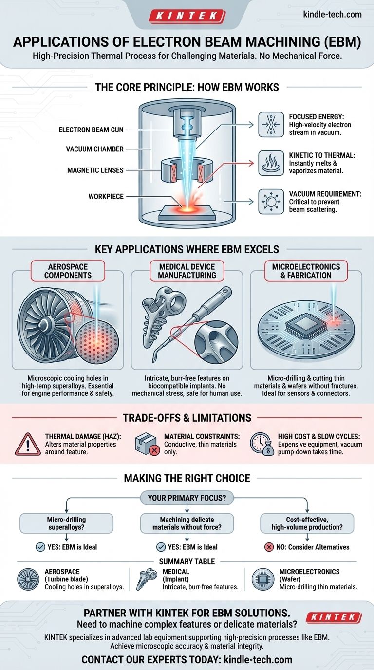
In essence, Electron Beam Machining (EBM) is a highly specialized thermal process used for precision drilling and cutting of materials that are difficult or impossible to machine using conventional methods. Its primary applications are found in industries requiring microscopic accuracy and the ability to work with advanced alloys, such as aerospace, medical device manufacturing, and microelectronics.
The core value of Electron Beam Machining is not speed or volume, but its unique ability to create extremely fine, complex features in hard-to-machine materials with no mechanical force, making it an indispensable tool for highly specialized manufacturing challenges.
How EBM Achieves Its Precision
The Core Principle: Focused Energy
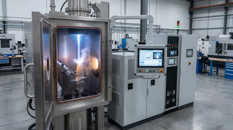
Electron Beam Machining operates by generating a stream of high-velocity electrons in a vacuum. This beam is then focused and directed onto the workpiece using magnetic lenses.
From Kinetic to Thermal Energy
When the concentrated beam of electrons strikes the material, their kinetic energy is instantly converted into intense thermal energy. This localized heating is so rapid and extreme that it melts and vaporizes the material in a very small, controlled area.
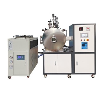
The Vacuum Requirement
The entire process must take place in a high-vacuum chamber. This is critical because it prevents the electrons from colliding with air molecules, which would scatter the beam and dissipate its energy before it reaches the workpiece.
Key Applications Where EBM Excels
Aerospace Components
EBM is fundamental for drilling microscopic cooling holes in jet engine turbine blades. These blades are made from high-temperature superalloys that are extremely difficult to machine mechanically. EBM can create thousands of precise holes, often at very shallow angles, which is vital for engine performance and safety.
Medical Device Manufacturing
In the medical field, EBM is used to create intricate and burr-free features on implants and surgical tools. Its ability to machine biocompatible materials like titanium with high precision and without introducing mechanical stress makes it ideal for producing complex components that are both durable and safe for human use.
Microelectronics and Fabrication
For the electronics industry, EBM provides a method for micro-drilling and cutting thin materials and silicon wafers. It can create microscopic slots and holes essential for sensors, connectors, and other micro-scale components where mechanical cutting would cause fractures or defects.
Understanding the Trade-offs and Limitations
Thermal Damage
While EBM exerts no mechanical force, it is a thermal process. This creates a small Heat Affected Zone (HAZ) around the machined feature, which can alter the material's microstructure and properties. This must be accounted for in the design.
Material and Thickness Constraints
EBM is most effective on materials with high thermal conductivity and is generally limited to thinner sections. The deeper the cut, the less efficient and precise the process becomes. It is also not suitable for non-conductive materials.
High Capital Cost and Slow Cycle Times
EBM systems are expensive to purchase and operate, requiring significant infrastructure for the vacuum chamber and high-voltage power supplies. The need to pump down the vacuum chamber for each cycle makes it a relatively slow process, unsuitable for high-volume production.
Making the Right Choice for Your Goal
- If your primary focus is micro-drilling in superalloys: EBM is a leading choice for creating fine, angled holes in materials that resist conventional drilling.
- If your primary focus is machining delicate, thin materials without force: Choose EBM to avoid the mechanical stress, burrs, and potential cracking associated with traditional cutting tools.
- If your primary focus is cost-effective, high-volume production: EBM is not the correct tool; its high cost and slow cycle times are prohibitive for mass manufacturing of simple parts.
Ultimately, selecting Electron Beam Machining is a strategic decision for applications where precision and the ability to machine difficult materials outweigh considerations of speed and cost.
Summary Table:
| Application Area | Key Use Case | Ideal For |
|---|---|---|
| Aerospace | Drilling microscopic cooling holes in turbine blades | Machining high-temperature superalloys |
| Medical Devices | Creating intricate, burr-free features on implants | Working with biocompatible materials like titanium |
| Microelectronics | Micro-drilling and cutting silicon wafers | Fabricating delicate, thin components without force |
Need to machine complex features in superalloys or delicate materials? KINTEK specializes in providing advanced lab equipment and consumables that support high-precision manufacturing processes like Electron Beam Machining. Whether you're in aerospace, medical device production, or microelectronics, our solutions help you achieve the microscopic accuracy and material integrity your projects demand. Contact our experts today to discuss how we can enhance your laboratory's capabilities and streamline your specialized manufacturing challenges.
Visual Guide
Related Products
- HFCVD Machine System Equipment for Drawing Die Nano-Diamond Coating
- Laboratory Test Sieves and Sieving Machines
- Anti-Cracking Press Mold for Lab Use
- CVD Diamond Cutting Tool Blanks for Precision Machining
- Benchtop Laboratory Vacuum Freeze Dryer
People Also Ask
- How is something diamond coated? A Guide to CVD Growth vs. Plating Methods
- How do CVD diamonds grow? A Step-by-Step Guide to Lab-Grown Diamond Creation
- What is direct current DC magnetron sputtering? A Guide to High-Quality Thin Film Deposition
- Is sputtering a PVD? Discover the Key Coating Technology for Your Lab
- How is diamond coating made? A Guide to CVD and PVD Methods