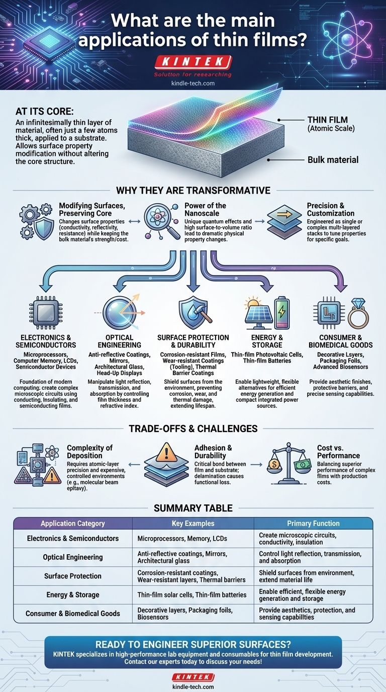
At its core, a thin film is an infinitesimally thin layer of material, often just a few atoms thick, applied to the surface of a substrate. This seemingly simple concept enables a vast array of modern technologies, with primary applications spanning electronics, optics, and protective coatings. You interact with thin films daily, from the anti-reflective coating on your eyeglasses and the screen of your smartphone to the components inside your computer and the protective layer on cutting tools.
The fundamental power of thin films is their ability to bestow entirely new properties—such as electrical conductivity, optical reflectivity, or chemical resistance—onto the surface of a bulk material without altering its core structure, enabling functionality that would otherwise be impossible or cost-prohibitive.
The Principle: Why Thin Films are Transformative
Before listing the applications, it's crucial to understand why these microscopic layers are so powerful. Their utility stems from a few key principles.
Modifying Surfaces, Preserving the Core
A thin film allows engineers to change the surface properties of an object while leaving the underlying bulk material untouched. This is incredibly efficient, allowing the use of a strong, cheap substrate (like glass or steel) while adding a high-performance surface layer that provides a specific function.
The Power of the Nanoscale
When materials are reduced to atomic-scale layers, their physical properties can change dramatically. This is due to an increased surface-to-volume ratio and quantum effects, leading to unique optical, electrical, and magnetic behaviors not seen in the bulk material.
Precision and Customization
Thin films are not one-size-fits-all. They can be engineered as a single homogeneous layer or as a complex, multi-layered stack. This structure can be periodic, random, or follow a set pattern, allowing for the precise tuning of properties to meet a specific goal.
Key Application Categories Explained
The unique properties of thin films have made them indispensable across numerous industries. We can group their primary applications into a few major categories.
Electronics and Semiconductors
This is arguably the most significant application area. The entire microelectronics industry is built on the precise deposition of thin films.
Applications include semiconductor devices, microprocessors, computer memory, and light crystal displays (LCDs). Each of these relies on complex stacks of conducting, insulating, and semiconducting films to create circuits at the microscopic level.
Optical Engineering
Thin films are masters at manipulating light. By carefully controlling the thickness and refractive index of one or more layers, it's possible to control how light is reflected, transmitted, or absorbed.
This is used for anti-reflective coatings on ophthalmic lenses and camera lenses, high-reflectivity mirrors for lamps and telescopes, and specialized coatings on architectural glass for thermal insulation. It also enables technology like automotive head-up displays.
Surface Protection and Durability
One of the most common uses for thin films is to protect a surface from its environment. These coatings act as a shield, dramatically extending the life of the underlying material.
Examples include protective films that prevent corrosion on metals, hard wear-resistant coatings on machine tools and drill bits, and thermal barrier coatings used in high-temperature environments like jet engines.
Energy and Storage
Modern energy solutions increasingly rely on thin film technology for efficiency and new form factors.
Thin-film photovoltaic cells offer a lightweight and sometimes flexible alternative to traditional silicon solar panels. Similarly, thin-film batteries are being developed for applications requiring small, integrated power sources.
Consumer and Biomedical Goods
Thin films are also used in applications you might see and use every day.
This includes thin decorative layers on jewelry or bathroom fittings, packaging foils that protect food from oxygen and moisture, and advanced biosensors where a specific film reacts to the presence of biological molecules.
Understanding the Trade-offs and Challenges
While incredibly useful, implementing thin film technology is not without its complexities. Objectively understanding these challenges is key to appreciating its role.
The Complexity of Deposition
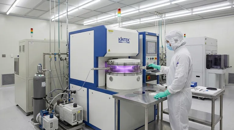
Creating a uniform, pure, and defect-free thin film is a highly technical process. Methods like molecular beam epitaxy deposit material one atomic layer at a time, requiring expensive equipment and highly controlled environments.
Adhesion and Durability
The bond between the thin film and the substrate is critical. If a film flakes, peels, or scratches off easily (a process called delamination), its function is lost. Ensuring strong adhesion is a primary challenge in materials science.
Cost vs. Performance
There is always a trade-off between the performance of a thin film and the cost of its production. A complex, multi-layered optical coating may offer superior performance, but its manufacturing cost might be prohibitive for a low-cost consumer product.
Making the Right Choice for Your Goal
Applying thin film technology effectively means aligning its capabilities with a specific functional outcome.
- If your primary focus is performance and miniaturization: You will leverage thin films in electronics, where precise layering of materials is the foundation of all modern computing.
- If your primary focus is manipulating light: Optical coatings are your domain, used for everything from enhancing camera lenses to improving the thermal efficiency of buildings.
- If your primary focus is durability and longevity: Protective coatings are essential, providing corrosion, wear, and thermal resistance to extend the life of critical components.
- If your primary focus is energy innovation: You will explore thin-film photovoltaics and batteries, which offer new form factors for efficient energy generation and storage.
Ultimately, thin film technology is a foundational tool for engineering the material surfaces that define and enable our modern world.
Summary Table:
| Application Category | Key Examples | Primary Function |
|---|---|---|
| Electronics & Semiconductors | Microprocessors, Memory, LCDs | Create microscopic circuits, conductivity, insulation |
| Optical Engineering | Anti-reflective coatings, Mirrors, Architectural glass | Control light reflection, transmission, and absorption |
| Surface Protection | Corrosion-resistant coatings, Wear-resistant layers, Thermal barriers | Shield surfaces from environment, extend material life |
| Energy & Storage | Thin-film solar cells, Thin-film batteries | Enable efficient, flexible energy generation and storage |
| Consumer & Biomedical Goods | Decorative layers, Packaging foils, Biosensors | Provide aesthetics, protection, and sensing capabilities |
Ready to engineer superior surfaces for your products? KINTEK specializes in high-performance lab equipment and consumables for developing and testing advanced thin films. Whether you're innovating in electronics, optics, or protective coatings, our solutions help you achieve precise, durable, and efficient results. Contact our experts today to discuss how we can support your laboratory's thin film research and production needs.
Visual Guide
Related Products
- Aluminized Ceramic Evaporation Boat for Thin Film Deposition
- Tungsten Evaporation Boat for Thin Film Deposition
- Electron Beam Evaporation Coating Oxygen-Free Copper Crucible and Evaporation Boat
- Molybdenum Tungsten Tantalum Evaporation Boat for High Temperature Applications
- Aluminum-Plastic Flexible Packaging Film for Lithium Battery Packaging
People Also Ask
- What are the alternatives to sputtering? Choose the Right Thin Film Deposition Method
- What is the source of evaporation for thin film? Choosing Between Thermal and E-Beam Methods
- Why is an alumina boat selected for catalyst precursors? Ensure Sample Purity at 1000 °C
- Why are high-purity ceramic boats used for lignin activation? Ensure Purity & Thermal Stability
- What is the chemical method for thin film deposition? Build Films from the Molecular Level Up


