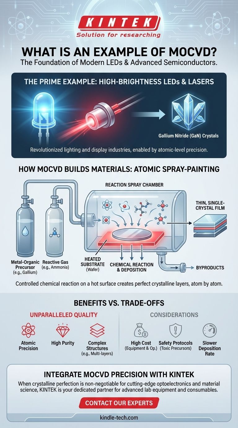
By far, the most prevalent example of Metal-Organic Chemical Vapor Deposition (MOCVD) is the manufacturing of high-brightness Light Emitting Diodes (LEDs) and semiconductor lasers. This process is particularly critical for producing the gallium nitride (GaN) crystals that are the foundation of modern blue, green, and white LEDs, which have revolutionized the lighting and display industries.
MOCVD is not merely a manufacturing technique; it is a foundational process for creating the high-purity, complex crystalline materials required by virtually all modern high-performance semiconductor devices. Its defining feature is the ability to build these materials with atomic-level precision.
How MOCVD Builds Advanced Materials
MOCVD is a highly controlled process for depositing thin, single-crystal films onto a substrate. Think of it as a form of "atomic spray-painting" where individual atomic layers are built up to create a perfect, functional material.
The Core Principle: Chemical Reaction on a Hot Surface
At its heart, the MOCVD process involves introducing specific precursor gases into a reaction chamber containing a heated substrate (a wafer). When these gases flow over the hot wafer, they decompose in a controlled chemical reaction.
This reaction leaves behind a thin, solid film of the desired material on the wafer's surface, while the unwanted byproducts are exhausted from the chamber.
The Role of "Metal-Organic" Precursors
The name "Metal-Organic" refers to the precursor gases used. To deposit a material like gallium nitride (GaN), you need to deliver gallium atoms and nitrogen atoms to the wafer.
The "metal" component, such as gallium, is bonded to an organic molecule. This organic attachment makes the metal compound volatile, allowing it to be transported as a gas. The nitrogen is typically supplied by a simpler gas, like ammonia.
When these precursors react at the hot surface, the organic molecules and other byproducts are released, leaving behind only the pure, intended material like GaN in a perfect crystalline layer.
The Result: High-Quality Crystalline Films
This precise, layer-by-layer deposition is what makes MOCVD so powerful. It allows engineers to create highly conformal films with superior electrical and thermal properties.
This level of control is essential for fabricating the complex multi-layer structures found in lasers, high-frequency transistors, and high-efficiency solar cells.
Understanding the Trade-offs of MOCVD
While incredibly powerful, MOCVD is a specialized process with distinct trade-offs that make it suitable for high-value applications but less so for others.
High Cost and Complexity
MOCVD reactors are sophisticated and expensive pieces of equipment. They must maintain ultra-high vacuum, precise temperature control, and extremely pure gas flows, all of which contribute to high capital and operational costs.
Precursor Handling and Safety
The metal-organic precursors are often toxic, flammable, or even pyrophoric (igniting spontaneously in air). This requires stringent safety protocols and specialized handling infrastructure, further adding to the complexity and cost.
Slower Deposition Rates
Because MOCVD is designed for atomic-level precision, its deposition rate can be slower than other, less precise bulk-film deposition methods. The trade-off is sacrificing speed to achieve unparalleled material quality and purity.
Making the Right Choice for Your Goal
MOCVD is the industry standard for a specific class of problems. You choose it when the material's crystalline perfection is non-negotiable.
- If your primary focus is cutting-edge performance: MOCVD is essential for fabricating high-frequency GaN transistors or high-efficiency LEDs and lasers that require perfect crystal structures.
- If your primary focus is creating complex material stacks: For devices like multi-junction solar cells or laser diodes that depend on stacking different semiconductor materials flawlessly, MOCVD's atomic-level control is indispensable.
- If your primary focus is simple, low-cost film deposition: For applications that do not require perfect crystallinity, other methods like physical vapor deposition (sputtering or evaporation) are often faster and more cost-effective.
Ultimately, MOCVD is the technology of choice when the performance of the final device is limited by the purity and perfection of its foundational materials.
Summary Table:
| Aspect | Key Takeaway |
|---|---|
| Primary Example | Manufacturing of high-brightness LEDs (blue, green, white) and semiconductor lasers. |
| Key Material | Deposits high-purity gallium nitride (GaN) crystals. |
| Core Principle | Uses metal-organic precursor gases to build thin films atom-by-layer on a heated substrate. |
| Best For | Applications requiring perfect crystalline structures, like advanced optoelectronics. |
| Trade-offs | High cost, complexity, and slower deposition rates compared to other methods. |
Ready to Integrate MOCVD Precision into Your Lab?
If your research or production demands the unparalleled material quality and atomic-level control that Metal-Organic Chemical Vapor Deposition provides, KINTEK is your dedicated partner. We specialize in supplying the advanced lab equipment and consumables that laboratories need to push the boundaries in optoelectronics, semiconductor research, and material science.
Let us help you achieve the crystalline perfection required for cutting-edge devices. Contact our experts today to discuss your specific application requirements.
Visual Guide
Related Products
- Multi Heating Zones CVD Tube Furnace Machine Chemical Vapor Deposition Chamber System Equipment
- 915MHz MPCVD Diamond Machine Microwave Plasma Chemical Vapor Deposition System Reactor
- Microwave Plasma Chemical Vapor Deposition MPCVD Machine System Reactor for Lab and Diamond Growth
- Cylindrical Resonator MPCVD Machine System Reactor for Microwave Plasma Chemical Vapor Deposition and Lab Diamond Growth
- Molybdenum Vacuum Heat Treat Furnace
People Also Ask
- How does a CVD tube furnace inhibit the sintering of silver supports? Boost Membrane Durability and Performance
- What are the advantages of a multi-zone tube furnace for Sb2S3? Unlock Superior Semiconductor Thin Film Purity
- What advantages do CVD furnaces offer for Wf/W composites? Preserving Fiber Ductility and Interface Integrity
- What is the difference between hot wall CVD and cold wall CVD? Choose the Right System for Your Process
- What is the application of CVD in nanotechnology? Harness Atomic-Level Precision for Next-Gen Materials