Knowledge cvd machine What is chemical vapor deposition process semiconductor? Building the Microscopic Layers of Modern Chips
Author avatar

Tech Team · Kintek Solution

Updated 2 months ago

What is chemical vapor deposition process semiconductor? Building the Microscopic Layers of Modern Chips


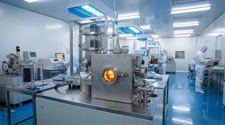
At its core, Chemical Vapor Deposition (CVD) is a manufacturing process for growing extremely thin, high-quality solid films on a surface. In semiconductor fabrication, this involves introducing carefully selected reactive gases into a vacuum chamber containing silicon wafers. These gases undergo a controlled chemical reaction, depositing a new, solid layer that becomes a fundamental building block of the final microchip.

Understanding Chemical Vapor Deposition is not just about coating a surface; it's about understanding how the microscopic, multi-layered cities inside a computer chip are constructed, layer by precise layer, by transforming gas into solid material.

What is chemical vapor deposition process semiconductor? Building the Microscopic Layers of Modern Chips

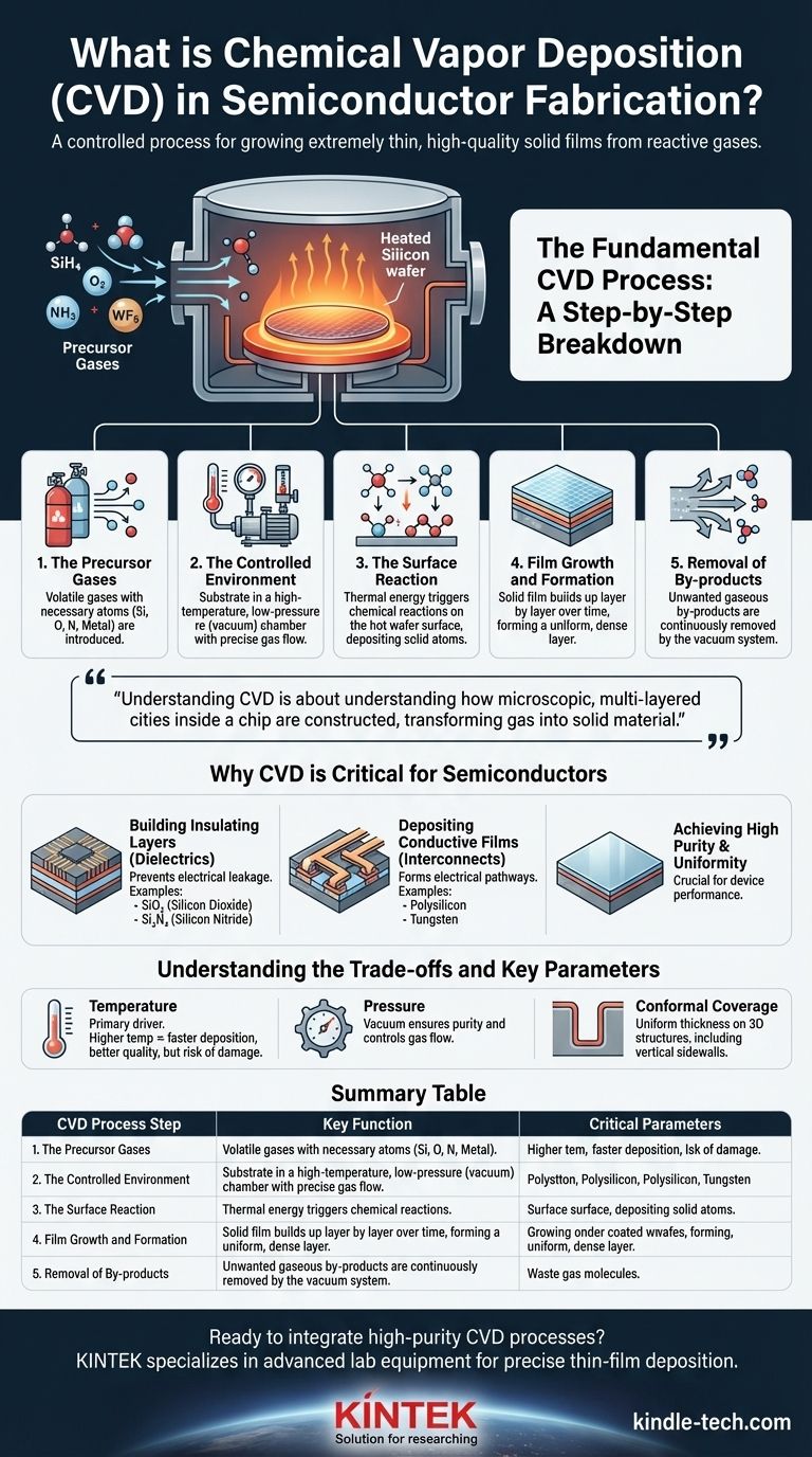
The Fundamental CVD Process: A Step-by-Step Breakdown

To truly grasp CVD, it's best to visualize it as a controlled, high-temperature construction process where the building materials arrive as a gas.

The Precursor Gases

The process begins with one or more volatile gases, known as precursors. These gases are specifically chosen because they contain the atoms needed for the final film (e.g., silicon, oxygen, nitrogen, or a metal).

The Controlled Environment

The silicon wafer, or substrate, is placed inside a reaction chamber. This chamber's environment is tightly controlled for three key variables: high temperature, low pressure (vacuum), and a precise gas flow rate.

The Surface Reaction

When the precursor gases flow over the heated substrate, the thermal energy triggers a chemical reaction. The gases decompose or react with each other directly on the hot surface of the wafer.

This reaction causes the desired atoms to "precipitate" out of their gaseous state and bond firmly to the substrate, forming a new solid layer.

Film Growth and Formation

This deposition process is not instantaneous. The solid film builds up over time, often atom by atom, growing into a uniform, dense layer across the entire wafer. The thickness is controlled by the duration of the process.

Removal of By-products

The chemical reaction almost always creates unwanted gaseous by-products. These volatile waste products are continuously removed from the chamber by the vacuum system's gas flow, leaving only the pure, solid film behind.

Why CVD is Critical for Semiconductors

CVD isn't just one of many options; it is an essential technique used repeatedly during the fabrication of a single chip to build different parts of its intricate circuitry.

Building Insulating Layers

Circuits require insulators to prevent electrical current from leaking between wires. CVD is the primary method for depositing high-purity insulating films, such as silicon dioxide (SiO₂) and silicon nitride (Si₃N₄).

Depositing Conductive Films

The "wires" that connect transistors are also often created using CVD. It is used to deposit films of polysilicon (a form of silicon) and various metals like tungsten, which serve as conductive pathways in the integrated circuit.

Achieving High Purity and Uniformity

The performance of a semiconductor device is critically dependent on the quality of its layers. CVD allows for exceptional control over the purity and thickness of the deposited film, ensuring consistent performance across the entire wafer.

Understanding the Trade-offs and Key Parameters

The success of a CVD process depends on a delicate balance of competing factors. Engineers must manage these variables to achieve the desired outcome.

The Role of Temperature

Temperature is the primary driver of the chemical reaction. Higher temperatures generally lead to faster deposition rates and higher quality films. However, excessive heat can damage the delicate structures already built on the chip in previous steps.

The Impact of Pressure

Operating under a vacuum is non-negotiable. The vacuum environment ensures purity by removing unwanted air molecules and helps control the flow of the precursor gases. Different pressures are used to influence the film's final properties and how evenly it coats the surface.

The Challenge of Conformal Coverage

As chips become more three-dimensional, a key challenge is ensuring the deposited film is equally thick on vertical sidewalls as it is on horizontal surfaces. This property, known as conformality, is a critical parameter that CVD is uniquely capable of controlling.

Making the Right Choice for Your Goal

The specific goals of your fabrication step dictate the ideal approach to CVD.

  • If your primary focus is creating a flawless insulating layer (dielectric): You need a process that guarantees exceptional uniformity and purity, as even microscopic defects can cause circuit failure.
  • If your primary focus is forming conductive pathways (interconnects): Your priority is achieving excellent adhesion to the underlying layer and the precise electrical properties required for the circuit.
  • If your primary focus is coating complex, three-dimensional structures: You must prioritize a CVD variant known for high conformality, ensuring the film is equally thick on all exposed surfaces.

Ultimately, mastering CVD is mastering the ability to construct the intricate, multi-layered architecture that defines modern electronics.

Summary Table:

CVD Process Step Key Function Critical Parameters
Precursor Gases Supply atoms (e.g., Si, O, N) for the film Gas composition, purity
Controlled Environment Enable the chemical reaction Temperature, pressure, gas flow rate
Surface Reaction Decompose gases to deposit solid film Substrate temperature
Film Growth Build a uniform, dense layer Process duration
By-product Removal Maintain film purity Vacuum system efficiency

Ready to integrate high-purity CVD processes into your semiconductor fabrication? KINTEK specializes in providing the advanced lab equipment and consumables essential for precise thin-film deposition. Our solutions help you achieve the uniform, conformal coatings critical for next-generation microchips. Contact our experts today to discuss how we can support your laboratory's specific semiconductor manufacturing goals.

Visual Guide

What is chemical vapor deposition process semiconductor? Building the Microscopic Layers of Modern Chips Visual Guide

Related Products

People Also Ask

Related Products

Chemical Vapor Deposition CVD Equipment System Chamber Slide PECVD Tube Furnace with Liquid Gasifier PECVD Machine

Chemical Vapor Deposition CVD Equipment System Chamber Slide PECVD Tube Furnace with Liquid Gasifier PECVD Machine

KT-PE12 Slide PECVD System: Wide power range, programmable temp control, fast heating/cooling with sliding system, MFC mass flow control & vacuum pump.

Microwave Plasma Chemical Vapor Deposition MPCVD Machine System Reactor for Lab and Diamond Growth

Microwave Plasma Chemical Vapor Deposition MPCVD Machine System Reactor for Lab and Diamond Growth

Get high-quality diamond films with our Bell-jar Resonator MPCVD machine designed for lab and diamond growth. Discover how Microwave Plasma Chemical Vapor Deposition works for growing diamonds using carbon gas and plasma.

915MHz MPCVD Diamond Machine Microwave Plasma Chemical Vapor Deposition System Reactor

915MHz MPCVD Diamond Machine Microwave Plasma Chemical Vapor Deposition System Reactor

915MHz MPCVD Diamond Machine and its multi-crystal effective growth, the maximum area can reach 8 inches, the maximum effective growth area of single crystal can reach 5 inches. This equipment is mainly used for the production of large-size polycrystalline diamond films, the growth of long single crystal diamonds, the low-temperature growth of high-quality graphene, and other materials that require energy provided by microwave plasma for growth.

Customer Made Versatile CVD Tube Furnace Chemical Vapor Deposition Chamber System Equipment

Customer Made Versatile CVD Tube Furnace Chemical Vapor Deposition Chamber System Equipment

Get your exclusive CVD furnace with KT-CTF16 Customer Made Versatile Furnace. Customizable sliding, rotating, and tilting functions for precise reactions. Order now!

HFCVD Machine System Equipment for Drawing Die Nano-Diamond Coating

HFCVD Machine System Equipment for Drawing Die Nano-Diamond Coating

The nano-diamond composite coating drawing die uses cemented carbide (WC-Co) as the substrate, and uses the chemical vapor phase method ( CVD method for short ) to coat the conventional diamond and nano-diamond composite coating on the surface of the inner hole of the mold.

Split Chamber CVD Tube Furnace with Vacuum Station Chemical Vapor Deposition System Equipment Machine

Split Chamber CVD Tube Furnace with Vacuum Station Chemical Vapor Deposition System Equipment Machine

Efficient split chamber CVD furnace with vacuum station for intuitive sample checking and quick cooling. Up to 1200℃ max temperature with accurate MFC mass flowmeter control.

RF PECVD System Radio Frequency Plasma-Enhanced Chemical Vapor Deposition RF PECVD

RF PECVD System Radio Frequency Plasma-Enhanced Chemical Vapor Deposition RF PECVD

RF-PECVD is an acronym for "Radio Frequency Plasma-Enhanced Chemical Vapor Deposition." It deposits DLC (Diamond-like carbon film) on germanium and silicon substrates. It is utilized in the 3-12um infrared wavelength range.

Multi Heating Zones CVD Tube Furnace Machine Chemical Vapor Deposition Chamber System Equipment

Multi Heating Zones CVD Tube Furnace Machine Chemical Vapor Deposition Chamber System Equipment

KT-CTF14 Multi Heating Zones CVD Furnace - Precise Temperature Control and Gas Flow for Advanced Applications. Max temp up to 1200℃, 4 channels MFC mass flow meter, and 7" TFT touch screen controller.

Cylindrical Resonator MPCVD Machine System Reactor for Microwave Plasma Chemical Vapor Deposition and Lab Diamond Growth

Cylindrical Resonator MPCVD Machine System Reactor for Microwave Plasma Chemical Vapor Deposition and Lab Diamond Growth

Learn about Cylindrical Resonator MPCVD Machine, the microwave plasma chemical vapor deposition method used for growing diamond gemstones and films in the jewelry and semi-conductor industries. Discover its cost-effective advantages over traditional HPHT methods.

Inclined Rotary Plasma Enhanced Chemical Vapor Deposition PECVD Equipment Tube Furnace Machine

Inclined Rotary Plasma Enhanced Chemical Vapor Deposition PECVD Equipment Tube Furnace Machine

Introducing our inclined rotary PECVD furnace for precise thin film deposition. Enjoy automatic matching source, PID programmable temperature control, and high accuracy MFC mass flowmeter control. Built-in safety features for peace of mind.

Inclined Rotary Plasma Enhanced Chemical Vapor Deposition PECVD Equipment Tube Furnace Machine

Inclined Rotary Plasma Enhanced Chemical Vapor Deposition PECVD Equipment Tube Furnace Machine

Upgrade your coating process with PECVD coating equipment. Ideal for LED, power semiconductors, MEMS and more. Deposits high-quality solid films at low temps.

Custom CVD Diamond Coating for Lab Applications

Custom CVD Diamond Coating for Lab Applications

CVD Diamond Coating: Superior Thermal Conductivity, Crystal Quality, and Adhesion for Cutting Tools, Friction, and Acoustic Applications

CVD Diamond for Thermal Management Applications

CVD Diamond for Thermal Management Applications

CVD diamond for thermal management: High-quality diamond with thermal conductivity up to 2000 W/mK, ideal for heat spreaders, laser diodes, and GaN on Diamond (GOD) applications.

CVD Diamond Dressing Tools for Precision Applications

CVD Diamond Dressing Tools for Precision Applications

Experience the Unbeatable Performance of CVD Diamond Dresser Blanks: High Thermal Conductivity, Exceptional Wear Resistance, and Orientation Independence.

CVD Diamond Cutting Tool Blanks for Precision Machining

CVD Diamond Cutting Tool Blanks for Precision Machining

CVD Diamond Cutting Tools: Superior Wear Resistance, Low Friction, High Thermal Conductivity for Non-Ferrous Materials, Ceramics, Composites Machining

Laboratory CVD Boron Doped Diamond Materials

Laboratory CVD Boron Doped Diamond Materials

CVD boron-doped diamond: A versatile material enabling tailored electrical conductivity, optical transparency, and exceptional thermal properties for applications in electronics, optics, sensing, and quantum technologies.

Electron Beam Evaporation Coating Oxygen-Free Copper Crucible and Evaporation Boat

Electron Beam Evaporation Coating Oxygen-Free Copper Crucible and Evaporation Boat

Electron Beam Evaporation Coating Oxygen-Free Copper Crucible enables precise co-deposition of various materials. Its controlled temperature and water-cooled design ensure pure and efficient thin film deposition.

Molybdenum Tungsten Tantalum Evaporation Boat for High Temperature Applications

Molybdenum Tungsten Tantalum Evaporation Boat for High Temperature Applications

Evaporation boat sources are used in thermal evaporation systems and are suitable for depositing various metals, alloys and materials. Evaporation boat sources are available in different thicknesses of tungsten, tantalum and molybdenum to ensure compatibility with a variety of power sources. As a container, it is used for vacuum evaporation of materials. They can be used for thin film deposition of various materials, or designed to be compatible with techniques such as electron beam fabrication.

Hemispherical Bottom Tungsten Molybdenum Evaporation Boat

Hemispherical Bottom Tungsten Molybdenum Evaporation Boat

Used for gold plating, silver plating, platinum, palladium, suitable for a small amount of thin film materials. Reduce the waste of film materials and reduce heat dissipation.

Vacuum Cold Mounting Machine for Sample Preparation

Vacuum Cold Mounting Machine for Sample Preparation

Vacuum Cold Mounting Machine for precise sample prep. Handles porous, fragile materials with -0.08MPa vacuum. Ideal for electronics, metallurgy, and failure analysis.


Leave Your Message