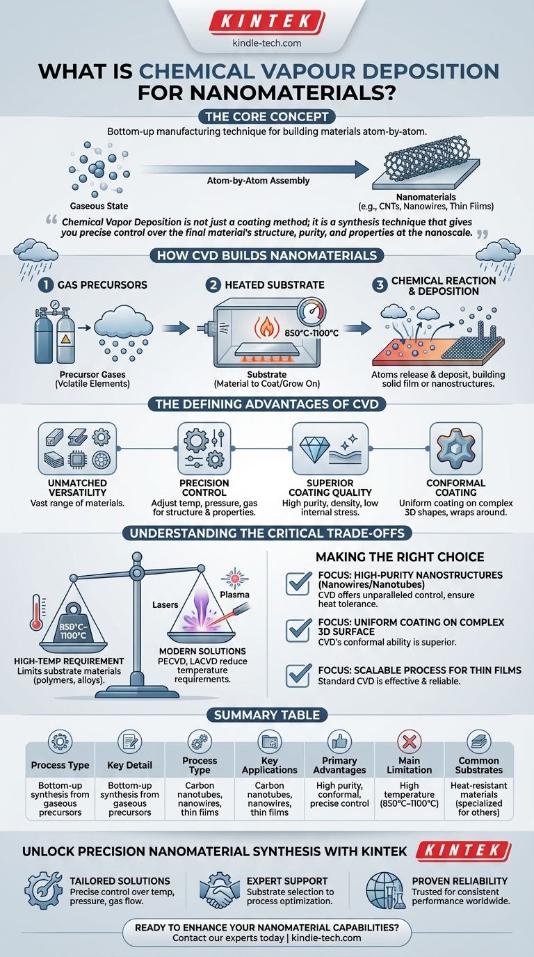
At its core, Chemical Vapor Deposition (CVD) is a highly controlled process for building materials atom-by-atom from a gaseous state. For nanomaterials, this means it is a "bottom-up" manufacturing technique used to grow structures like carbon nanotubes and nanowires, or to deposit exceptionally thin, high-performance films on a surface.
Chemical Vapor Deposition is not just a coating method; it is a synthesis technique that gives you precise control over the final material's structure, purity, and properties at the nanoscale, making it a cornerstone of modern electronics and materials science.
How CVD Builds Nanomaterials from the Ground Up
To understand CVD, think of it as a controlled "rain" of specific atoms onto a heated surface. Instead of water, the "clouds" are chemical precursor gases, and the "rain" is a solid material that forms precisely where you want it.
The Gaseous Precursors
The process begins by introducing one or more volatile precursor gases into a reaction chamber. These gases contain the chemical elements you want to deposit.
The Heated Substrate
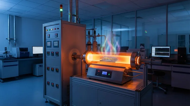
Inside the chamber is a substrate, which is the material you want to coat or grow your nanomaterial on. This substrate is heated to a specific, often very high, temperature.
The Chemical Reaction and Deposition
When the precursor gases come into contact with the hot substrate, they undergo a chemical reaction or decompose. The atoms of the desired material are released and "deposit" onto the surface, gradually building a solid film or growing into specific nanostructures.
The Defining Advantages of CVD
The reason CVD is so widely used is because it offers a unique combination of versatility and precision, which is critical when working at the nanoscale.
Unmatched Versatility in Materials
CVD is not limited to one type of material. It can be used to deposit a vast range of materials, including metals, semiconductors (like those for electronics), and ceramics (for wear-resistant coatings).
Precision Control Over Structure
By carefully adjusting parameters like temperature, pressure, and gas composition, you can dictate the final properties of the material. This includes its chemical makeup, crystalline structure, grain size, and morphology.
Superior Coating Quality
The resulting films or nanostructures are typically of very high purity and density. This process also produces films with low internal stress and good crystallization, which are critical for high-performance applications like semiconductors.
Conformal Coating on Complex Shapes
Unlike methods that only coat what's in their direct line of sight, the gaseous nature of CVD allows it to "wrap around" complex, three-dimensional shapes, creating a perfectly uniform coating on all surfaces.
Understanding the Critical Trade-offs
No technique is without its limitations. True expertise lies in knowing both the strengths and the weaknesses of a process.
The High-Temperature Requirement
The most significant limitation of traditional CVD is its high reaction temperature, often between 850°C and 1100°C. Many important substrate materials, such as polymers or certain alloys, cannot withstand this heat without melting or degrading.
Modern Solutions to the Heat Problem
To overcome this, specialized variations of CVD have been developed. Techniques like Plasma-Enhanced CVD (PECVD) or Laser-Assisted CVD (LACVD) can significantly reduce the required deposition temperature, opening up compatibility with a wider range of substrates.
Making the Right Choice for Your Application
Choosing the right deposition technique depends entirely on your end goal. Here is how to decide if CVD is the correct path.
- If your primary focus is producing high-purity, crystalline nanostructures like nanowires or nanotubes: CVD offers unparalleled control over growth and structure, but you must ensure your substrate can handle the temperature.
- If your primary focus is applying a uniform, dense coating on a complex 3D surface: CVD's ability to create conformal films makes it a superior choice over line-of-sight methods like sputtering.
- If your primary focus is a scalable process for thin films on heat-resistant substrates: The relative simplicity and maintainability of standard CVD equipment can make it a highly effective and reliable manufacturing technique.
Ultimately, CVD provides a powerful toolkit for engineering materials from the nanoscale up, offering precision where it matters most.
Summary Table:
| Aspect | Key Detail |
|---|---|
| Process Type | Bottom-up synthesis from gaseous precursors |
| Key Applications | Carbon nanotubes, nanowires, thin films for electronics |
| Primary Advantages | High purity, conformal coating, precise structural control |
| Main Limitation | High temperature requirements (850°C–1100°C) |
| Common Substrates | Heat-resistant materials (specialized variants for polymers/alloys) |
Unlock Precision Nanomaterial Synthesis with KINTEK
Chemical Vapor Deposition is a cornerstone of advanced materials engineering—but achieving optimal results requires the right equipment and expertise. At KINTEK, we specialize in lab equipment and consumables tailored for cutting-edge nanotechnology applications.
Why choose KINTEK for your CVD needs?
- Tailored Solutions: Our CVD systems are designed for precise control over temperature, pressure, and gas flow—critical for growing high-quality nanomaterials.
- Expert Support: From substrate selection to process optimization, our team helps you navigate the complexities of nanomaterial synthesis.
- Proven Reliability: Trusted by laboratories worldwide for consistent performance in electronics, coatings, and materials research.
Ready to enhance your nanomaterial capabilities? Contact our experts today to discuss how our CVD solutions can advance your research or production goals.
Visual Guide
Related Products
- Chemical Vapor Deposition CVD Equipment System Chamber Slide PECVD Tube Furnace with Liquid Gasifier PECVD Machine
- Microwave Plasma Chemical Vapor Deposition MPCVD Machine System Reactor for Lab and Diamond Growth
- 915MHz MPCVD Diamond Machine Microwave Plasma Chemical Vapor Deposition System Reactor
- Customer Made Versatile CVD Tube Furnace Chemical Vapor Deposition Chamber System Equipment
- Split Chamber CVD Tube Furnace with Vacuum Station Chemical Vapor Deposition System Equipment Machine
People Also Ask
- How expensive is chemical vapor deposition? Understanding the True Cost of High-Performance Coating
- How are carbon nanotubes grown? Master Scalable Production with Chemical Vapor Deposition
- What is plasma enhanced chemical vapor deposition PECVD equipment? A Guide to Low-Temperature Thin Film Deposition
- What is the chemical vapor deposition growth process? Build Superior Thin Films from the Atom Up
- What are the core advantages of PE-CVD in OLED encapsulation? Protect Sensitive Layers with Low-Temp Film Deposition


