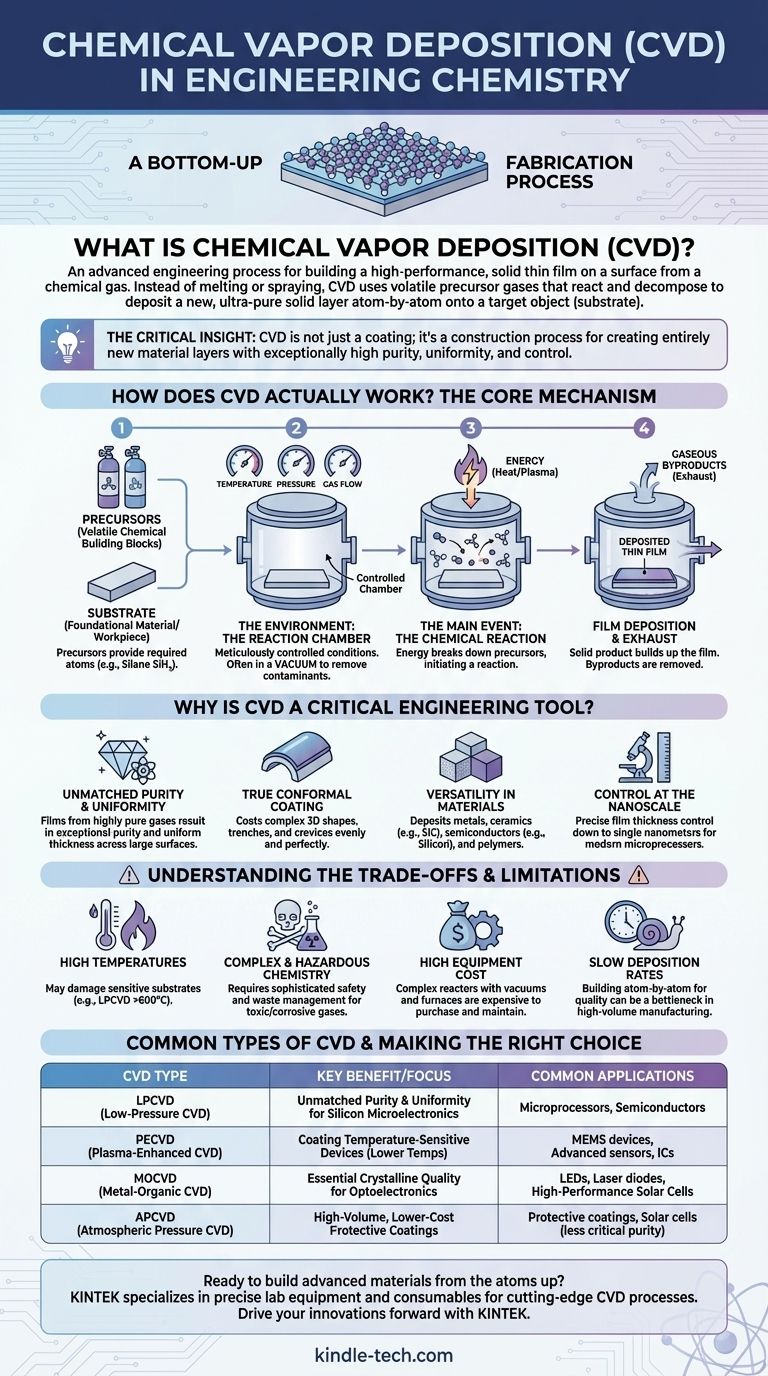
At its core, Chemical Vapor Deposition (CVD) is an advanced engineering process for building a high-performance, solid thin film on a surface from a chemical gas. Instead of melting and spraying a material, CVD uses volatile precursor gases that react and decompose in a controlled environment, depositing a new, ultra-pure solid layer atom-by-atom onto a target object, known as a substrate. This method is fundamental to modern manufacturing, especially in the electronics and materials science industries.
The crucial insight is that CVD is not merely a coating technique; it is a bottom-up fabrication process. It allows engineers to construct entirely new material layers with exceptional purity, uniformity, and control, enabling the creation of components that would be impossible to make by other means.
How Does CVD Actually Work? The Core Mechanism
Understanding CVD requires visualizing a precise, multi-stage process occurring within a controlled chamber. Each step is critical to the quality of the final film.
The Key Ingredients: Precursors and Substrate
The process begins with two main components. The substrate is the foundational material or workpiece that will receive the new layer.
The precursors are the chemical building blocks. These are volatile gases specifically chosen because they contain the atoms needed for the final film (e.g., silane gas, SiH₄, is a precursor for depositing pure silicon).
The Environment: The Reaction Chamber
This entire process takes place inside a sealed reaction chamber. The conditions inside—primarily temperature, pressure, and gas flow—are meticulously controlled.
For many CVD processes, a vacuum is created by pumping out the air. This removes contaminants and gives the precursor gas molecules a clear path to the substrate, a key factor for creating high-purity films.
The Main Event: The Chemical Reaction
Energy, typically in the form of high heat, is introduced into the chamber. This energy breaks down the precursor gases, initiating a chemical reaction.
The solid product of this reaction is then deposited onto the heated substrate, gradually building up the desired thin film. The gaseous byproducts of the reaction are then pumped out of the chamber as exhaust.
Why is CVD a Critical Engineering Tool?
The reason CVD is so ubiquitous in high-tech manufacturing is that it offers advantages that are difficult or impossible to achieve with conventional methods like electroplating or physical sputtering.
Unmatched Purity and Uniformity
Because the film is built from a highly pure gas, the resulting solid layer is also exceptionally pure. The nature of the gas deposition allows the film to be incredibly uniform in thickness, even across large surfaces like a silicon wafer.
True Conformal Coating
CVD excels at coating complex, three-dimensional shapes evenly. Imagine how fine dust settles perfectly over every contour of an intricate sculpture; CVD works similarly, ensuring that even trenches and crevices in a microchip are coated uniformly. This is known as conformal coating.
Versatility in Materials
The technique is remarkably versatile. Engineers can use CVD to deposit a vast range of materials, including highly pure metals, durable ceramics like silicon carbide, semiconductors like silicon, and even advanced polymers.
Control at the Nanoscale
The process is so precise that film thickness can be controlled down to the level of single nanometers. This level of control is absolutely essential for fabricating modern microprocessor components.
Understanding the Trade-offs and Limitations
While powerful, CVD is not a universal solution. Its application comes with significant technical challenges and trade-offs that engineers must manage.
High Temperatures Can Be a Problem
Many common CVD processes, such as LPCVD, require extremely high temperatures (often >600°C). This intense heat can damage or warp sensitive substrates, including certain electronics or plastics.
Complex and Hazardous Chemistry
The precursor gases are often highly toxic, flammable, or corrosive. This necessitates sophisticated safety systems, specialized handling procedures, and careful management of hazardous waste byproducts.
High Equipment Cost
CVD reactors are complex, precision instruments. The need for vacuum systems, high-temperature furnaces, and intricate gas handling makes the equipment expensive to purchase and maintain.
Deposition Rates Can Be Slow
Building a film atom-by-atom to achieve high quality can be a slow process. While this ensures precision, it can be a bottleneck in high-volume manufacturing scenarios.
Common Types of CVD Explained
To overcome specific limitations, engineers have developed several variations of the core CVD process.
LPCVD (Low-Pressure CVD)
This is a workhorse of the semiconductor industry. By operating at very low pressure, it reduces unwanted gas-phase reactions and improves the purity and uniformity of the deposited film. It typically requires high temperatures.
PECVD (Plasma-Enhanced CVD)
PECVD uses an electrical plasma to energize the precursor gases instead of relying solely on heat. This allows deposition to occur at much lower temperatures, making it ideal for coating temperature-sensitive materials like integrated circuits that have already been partially fabricated.
MOCVD (Metal-Organic CVD)
This specialized technique uses metal-organic compounds as precursors. MOCVD is critical for creating high-quality, complex crystalline films, and it is the dominant process for manufacturing high-brightness LEDs, lasers, and high-performance solar cells.
Making the Right Choice for Your Goal
Selecting the correct CVD method is entirely dependent on the material requirements, the substrate's limitations, and the desired outcome.
- If your primary focus is unmatched purity and uniformity for silicon-based microelectronics: LPCVD is the established industry standard.
- If your primary focus is coating a temperature-sensitive electronic device or polymer: PECVD is the necessary solution to avoid damaging the substrate.
- If your primary focus is manufacturing advanced optoelectronics like LEDs or laser diodes: MOCVD provides the essential crystalline quality needed for high performance.
- If your primary focus is a high-volume, lower-cost protective coating where ultimate purity is secondary: Simpler methods like Atmospheric Pressure CVD (APCVD) may be more practical.
By understanding these core principles, you can appreciate CVD as a foundational tool that empowers engineers to design and build advanced materials from the atoms up.
Summary Table:
| Feature | Key Benefit | Common Applications |
|---|---|---|
| Unmatched Purity | Creates high-performance solid layers from gas precursors. | Microprocessors, Semiconductors |
| Conformal Coating | Uniformly coats complex 3D shapes and trenches. | MEMS devices, Advanced sensors |
| Material Versatility | Deposits metals, ceramics, and polymers. | Protective coatings, Solar cells |
| Nanoscale Control | Enables precise film thickness down to nanometers. | LEDs, Laser diodes, Optoelectronics |
Ready to build advanced materials from the atoms up?
KINTEK specializes in providing the precise lab equipment and consumables needed for cutting-edge CVD processes. Whether you are developing new semiconductors, high-performance LEDs, or durable protective coatings, our solutions help you achieve the purity, uniformity, and control critical for success.
Contact our experts today to discuss how we can support your laboratory's specific CVD needs and drive your innovations forward.
Visual Guide
Related Products
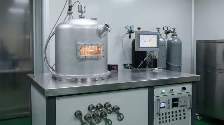
- Chemical Vapor Deposition CVD Equipment System Chamber Slide PECVD Tube Furnace with Liquid Gasifier PECVD Machine
- Customer Made Versatile CVD Tube Furnace Chemical Vapor Deposition Chamber System Equipment
- Microwave Plasma Chemical Vapor Deposition MPCVD Machine System Reactor for Lab and Diamond Growth
- 915MHz MPCVD Diamond Machine Microwave Plasma Chemical Vapor Deposition System Reactor
- Custom CVD Diamond Coating for Lab Applications
People Also Ask
- What are the core advantages of PE-CVD in OLED encapsulation? Protect Sensitive Layers with Low-Temp Film Deposition
- What are the processes of vapor phase deposition? Understand CVD vs. PVD for Superior Thin Films
- What types of substrates are used in CVD to facilitate graphene films? Optimize Graphene Growth with the Right Catalyst
- What is plasma enhanced chemical vapor deposition PECVD equipment? A Guide to Low-Temperature Thin Film Deposition
- How are carbon nanotubes grown? Master Scalable Production with Chemical Vapor Deposition


