Plasma Enhanced Chemical Vapor Deposition (PECVD) is a specialized vacuum deposition process used primarily in semiconductor manufacturing to coat substrates with thin films. Unlike traditional methods that rely on intense heat to trigger chemical reactions, PECVD utilizes electrical energy to generate plasma, allowing high-quality materials like silicon dioxide to be deposited at significantly lower temperatures.
Core Insight: The fundamental innovation of PECVD is the substitution of thermal energy with "energetic electrons." By using plasma to activate gases, manufacturers can deposit critical films without exposing delicate microchips to destructive heat levels.
The Mechanics of PECVD
Replacing Heat with Plasma
In standard Chemical Vapor Deposition (CVD), extreme heat is required to dissociate gases and form a solid film. PECVD fundamentally changes this dynamic by introducing plasma—an ionized gas containing free electrons and ions.
Energetic Electron Activation
Instead of heating the entire chamber to high temperatures, PECVD uses electromagnetic means, such as Radio Frequency (RF) or microwave excitation, to energize the gas. The energetic electrons within the plasma collide with the source gas molecules, breaking them apart (dissociation) to initiate the chemical reaction.
The Electrode Setup
The process typically occurs in a vacuum chamber containing parallel electrodes: one grounded and one RF-energized. The substrate (such as a silicon wafer) is placed on the electrode. The capacitive coupling between these plates excites the reactant gases into a glow discharge, creating the plasma necessary for deposition.
The Critical Advantage: Temperature Control
Operating within Strict Thermal Budgets
The primary driver for choosing PECVD is the need for low-temperature processing. While standard CVD often requires temperatures that can damage pre-existing layers on a chip, PECVD operates effectively between 100°C and 400°C.
Protecting the Substrate
This reduction in temperature is vital for modern semiconductor fabrication. It allows for the deposition of films onto substrates that contain temperature-sensitive materials, such as aluminum interconnects or polymers, which would melt or degrade under standard CVD conditions.
Enhancing Surface Activity
Even at these lower temperatures, the plasma does more than just break down gases. The ionized gas creates a "glow discharge" near the substrate surface. This improves surface activity and, combined with cathode sputtering effects, ensures the film adheres strongly to the device.
Understanding the Trade-offs
Batch Size and Throughput
While PECVD offers superior control over temperature, it often comes with a trade-off in manufacturing volume. The process typically handles a smaller batch of wafers at one time compared to some high-temperature furnace methods.
Equipment Complexity
The requirement for vacuum systems, RF generators, and precise pressure controls (typically 1 to 600 Pa) makes PECVD equipment complex. Maintaining the precise balance of gas flow, pressure, and plasma energy is critical to achieving uniform film thickness.
Making the Right Choice for Your Goal
To determine if PECVD is the correct solution for your fabrication needs, consider your specific constraints:
- If your primary focus is Substrate Integrity: Choose PECVD if your device contains materials that cannot withstand temperatures above 400°C, such as metal layers or polymers.
- If your primary focus is Film Quality at Low Heat: Select this method to deposit high-quality dielectrics like silicon dioxide without the stress-inducing thermal cycles of standard CVD.
- If your primary focus is High-Volume Bulk Coating: Evaluate if the smaller batch processing of PECVD creates a bottleneck, and consider if a higher-temperature thermal CVD process is viable for your specific material.
PECVD remains the industry standard for bridging the gap between high-quality film deposition and the delicate thermal limits of modern microelectronics.
Summary Table:
| Feature | PECVD (Plasma Enhanced) | Traditional Thermal CVD |
|---|---|---|
| Energy Source | RF/Microwave-generated Plasma | High Thermal Heat |
| Processing Temp | 100°C to 400°C | 600°C to 1100°C |
| Substrate Compatibility | Heat-sensitive (Aluminum, Polymers) | High-temperature resistant only |
| Core Advantage | Low thermal budget; high film quality | High throughput; dense film growth |
| Chamber Pressure | 1 to 600 Pa (Vacuum) | Atmospheric to Low Vacuum |
Elevate Your Semiconductor Fabrication with KINTEK Precision
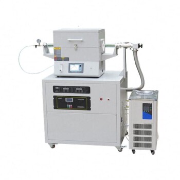
Are your delicate substrates reaching their thermal limits? KINTEK specializes in advanced laboratory solutions, offering high-performance PECVD systems and a comprehensive range of high-temperature furnaces, vacuum systems, and CVD equipment tailored for precision research and manufacturing.
Whether you are developing next-generation microelectronics or exploring battery research tools, our expert team provides the high-quality consumables—from PTFE products to specialized ceramics—and robust hardware needed to ensure uniform film thickness and superior material integrity.
Ready to optimize your deposition process? Contact KINTEK today for a consultation and custom quote!
Related Products
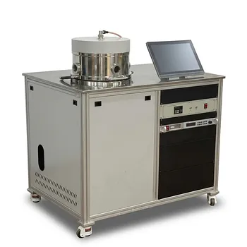
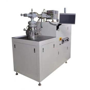
- RF PECVD System Radio Frequency Plasma-Enhanced Chemical Vapor Deposition RF PECVD
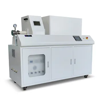
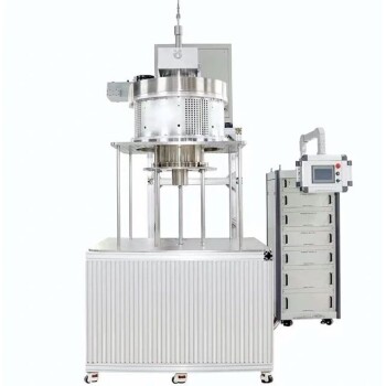
- Inclined Rotary Plasma Enhanced Chemical Vapor Deposition PECVD Equipment Tube Furnace Machine
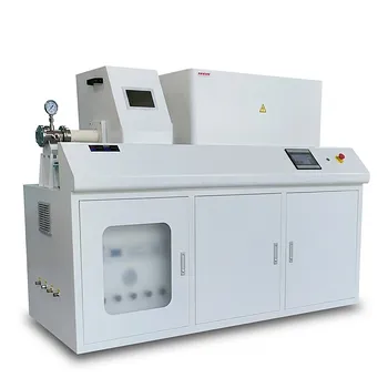
- Inclined Rotary Plasma Enhanced Chemical Vapor Deposition PECVD Equipment Tube Furnace Machine
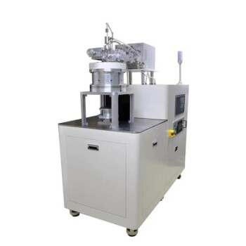
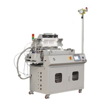
- Chemical Vapor Deposition CVD Equipment System Chamber Slide PECVD Tube Furnace with Liquid Gasifier PECVD Machine
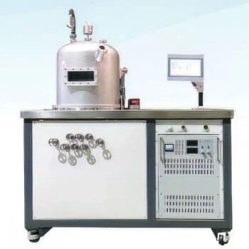
- Microwave Plasma Chemical Vapor Deposition MPCVD Machine System Reactor for Lab and Diamond Growth
People Also Ask
- What is an example of PECVD? RF-PECVD for High-Quality Thin Film Deposition
- How does Radio Frequency Enhanced Plasma Chemical Vapour Deposition (RF-PECVD) work? Learn the Core Principles
- What is plasma enhanced chemical Vapour deposition process used for fabrication of? A Guide to Low-Temperature Thin Films
- What is plasma enhanced chemical vapour deposition PECVD used for? Enable Low-Temp Thin Films for Electronics & Solar
- What is plasma chemical vapor deposition? A Low-Temperature Thin Film Coating Solution

