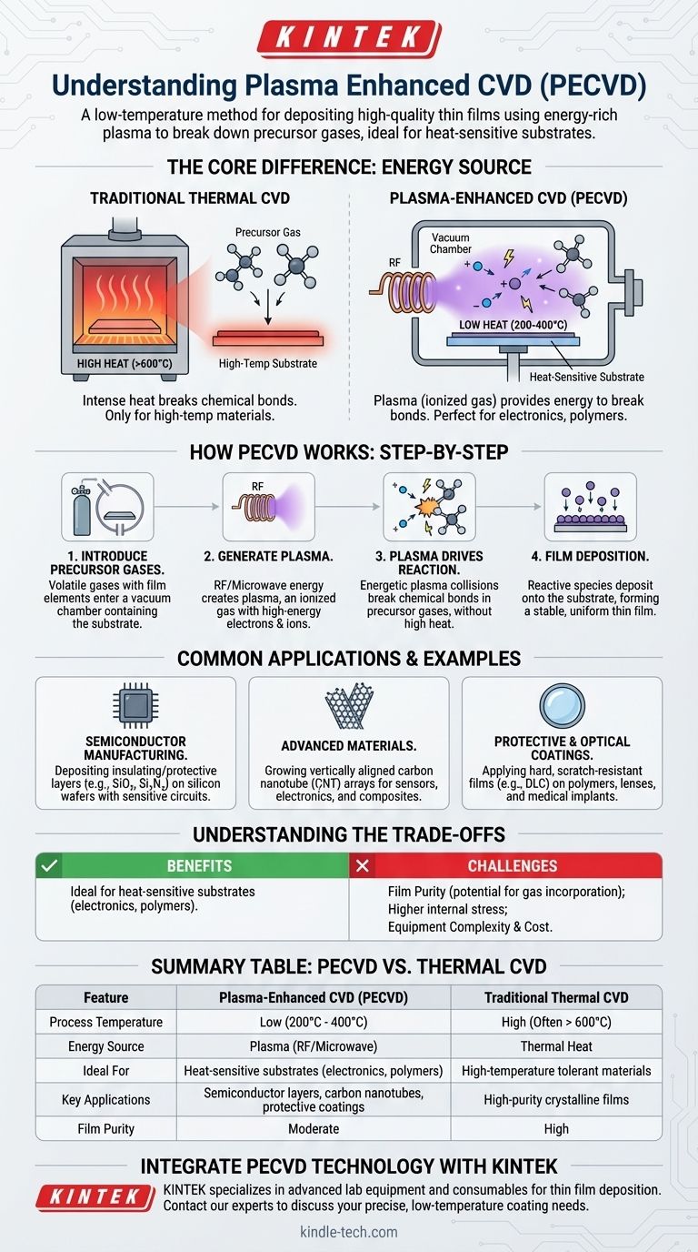
At its core, Plasma-Enhanced Chemical Vapor Deposition (PECVD) is a process used to deposit high-quality thin films onto a surface at much lower temperatures than traditional methods. It achieves this by using an energy-rich plasma to break down precursor gases and initiate the chemical reactions needed for deposition, rather than relying solely on high heat. This makes it ideal for coating materials that cannot withstand extreme temperatures.
The central advantage of PECVD is its ability to create durable, functional coatings on heat-sensitive materials. By substituting the intense heat of conventional Chemical Vapor Deposition (CVD) with the energy from a plasma, it opens up a range of applications for electronics, polymers, and other advanced components.
The Fundamentals: How Standard CVD Works
To understand what makes PECVD unique, we first must understand the baseline process it enhances: standard thermal Chemical Vapor Deposition (CVD).
Introducing Precursor Gases
The process begins by introducing one or more volatile precursor gases into a vacuum chamber containing the object to be coated, known as the substrate. These precursors contain the chemical elements that will form the final film.
The Role of High Temperature
In traditional thermal CVD, the chamber and substrate are heated to very high temperatures, often several hundred or even over a thousand degrees Celsius. This thermal energy is the catalyst that breaks the chemical bonds in the precursor gases.
Building the Film
Once broken down, the reactive chemical species deposit onto the hot substrate surface, forming a stable, solid, and highly uniform thin film. The volatile byproducts of the reaction are then pumped out of the chamber.
The "Plasma-Enhanced" Difference
PECVD follows the same basic principles but fundamentally changes how the reaction is powered, solving the primary limitation of thermal CVD.
The Problem with High Heat
The high temperatures required for thermal CVD can damage or destroy many useful substrates. This includes completed electronic circuits, plastics, and other materials with low melting points, severely limiting its applications.
Introducing Plasma: Energy Without Heat
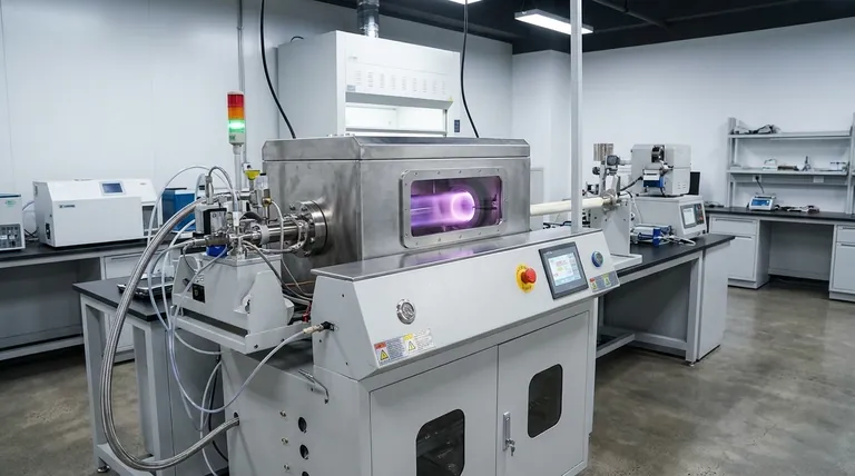
PECVD circumvents this problem by using plasma as the energy source. A plasma is an ionized gas, a state of matter created by applying a strong electromagnetic field (such as Radio Frequency or Microwave) to a gas at low pressure.
This process strips electrons from the gas atoms, creating a highly energetic mixture of ions and free electrons. This energy-rich environment exists without requiring extreme heat.
How Plasma Drives the Reaction
The energetic electrons and ions in the plasma collide with the precursor gas molecules. These collisions are powerful enough to break the chemical bonds—a task that normally requires high heat—and create the reactive species needed for deposition.
Because the reaction is driven by energetic plasma collisions instead of thermal vibration, the substrate can remain at a much lower temperature, often between 200°C and 400°C.
Common Applications and Examples
The lower processing temperature of PECVD makes it indispensable for manufacturing advanced materials and electronics.
Semiconductor Manufacturing
PECVD is widely used to deposit insulating and protective layers, such as silicon dioxide (SiO₂) and silicon nitride (Si₃N₄), onto silicon wafers that already contain sensitive electronic circuits. The low temperature prevents damage to the existing transistors and metal interconnects.
Advanced Materials (Carbon Nanotubes)
The process is also used to grow highly structured materials. For example, PECVD enables the growth of vertically aligned carbon nanotube (CNT) arrays on a substrate, a critical step for developing next-generation sensors, electronics, and composites.
Protective & Optical Coatings
PECVD can deposit hard, scratch-resistant films like diamond-like carbon (DLC) onto temperature-sensitive substrates like polymer lenses or medical implants, improving durability without damaging the underlying material.
Understanding the Trade-offs
Like any technology, PECVD has a specific set of advantages and challenges that make it suitable for some applications but not others.
Benefit: Temperature Sensitivity
The single greatest advantage is its ability to deposit films on substrates that cannot tolerate high heat. This is its primary purpose and the reason for its development.
Challenge: Film Purity and Stress
Because the reaction occurs in a complex plasma environment, atoms from the plasma gas (like hydrogen or argon) can become incorporated into the film, reducing its purity. Films can also have higher internal stress compared to those grown at high temperatures, which requires careful process tuning to manage.
Challenge: Equipment Complexity
A PECVD system requires sophisticated vacuum pumps, gas handling, and a power source (typically RF or microwave) to generate and sustain the plasma. This makes the equipment more complex and expensive than a simple thermal CVD furnace.
Making the Right Choice for Your Goal
Selecting a deposition method requires aligning the process capabilities with your primary objective for the thin film.
- If your primary focus is depositing on heat-sensitive substrates like integrated circuits or polymers: PECVD is the clear and often only choice due to its low-temperature processing.
- If your primary focus is achieving the highest possible film purity and crystalline perfection: High-temperature thermal CVD may be superior, provided your substrate can survive the intense heat.
- If your primary focus is creating highly conformal coatings inside complex, high-aspect-ratio structures: A different technique like Atomic Layer Deposition (ALD) might be more suitable.
Understanding the role of plasma as an energy source is the key to selecting the ideal deposition strategy for your specific material and application needs.
Summary Table:
| Feature | Plasma-Enhanced CVD (PECVD) | Traditional Thermal CVD |
|---|---|---|
| Process Temperature | Low (200°C - 400°C) | High (Often > 600°C) |
| Energy Source | Plasma (RF/Microwave) | Thermal Heat |
| Ideal For | Heat-sensitive substrates (electronics, polymers) | High-temperature tolerant materials |
| Key Applications | Semiconductor layers, carbon nanotubes, protective coatings | High-purity crystalline films |
| Film Purity | Moderate (potential for gas incorporation) | High |
Ready to integrate PECVD technology into your lab workflow? KINTEK specializes in advanced lab equipment and consumables for thin film deposition and materials science. Whether you're working with sensitive electronics, polymers, or developing next-generation materials like carbon nanotubes, our expertise and solutions can help you achieve precise, low-temperature coatings. Contact our experts today to discuss how we can support your specific laboratory needs and enhance your research capabilities.
Visual Guide
Related Products
- RF PECVD System Radio Frequency Plasma-Enhanced Chemical Vapor Deposition RF PECVD
- Chemical Vapor Deposition CVD Equipment System Chamber Slide PECVD Tube Furnace with Liquid Gasifier PECVD Machine
- Inclined Rotary Plasma Enhanced Chemical Vapor Deposition PECVD Equipment Tube Furnace Machine
- Microwave Plasma Chemical Vapor Deposition MPCVD Machine System Reactor for Lab and Diamond Growth
- Inclined Rotary Plasma Enhanced Chemical Vapor Deposition PECVD Equipment Tube Furnace Machine
People Also Ask
- Why is a Matching Network Indispensable in RF-PECVD for Siloxane Films? Ensure Stable Plasma and Uniform Deposition
- What is plasma enhanced chemical vapour deposition process? Unlock Low-Temperature, High-Quality Thin Films
- How does Radio Frequency Enhanced Plasma Chemical Vapour Deposition (RF-PECVD) work? Learn the Core Principles
- What is the role of RF-PECVD in VFG preparation? Mastering Vertical Growth and Surface Functionality
- How does plasma enhance CVD? Unlock Low-Temperature, High-Quality Film Deposition


