In materials science and manufacturing, sputtering is a physical vapor deposition (PVD) method used to create exceptionally thin and uniform films of material. The process works by ejecting atoms from a source material, known as a "target," by bombarding it with high-energy ions inside a vacuum chamber. These ejected atoms then travel and deposit onto a substrate, gradually building a new material layer with highly controlled properties.
Sputtering is fundamentally a process of momentum exchange. It uses an energized gas plasma to create a stream of ions that act like a microscopic sandblaster, precisely chipping atoms off a target material and redepositing them to form a high-performance coating.
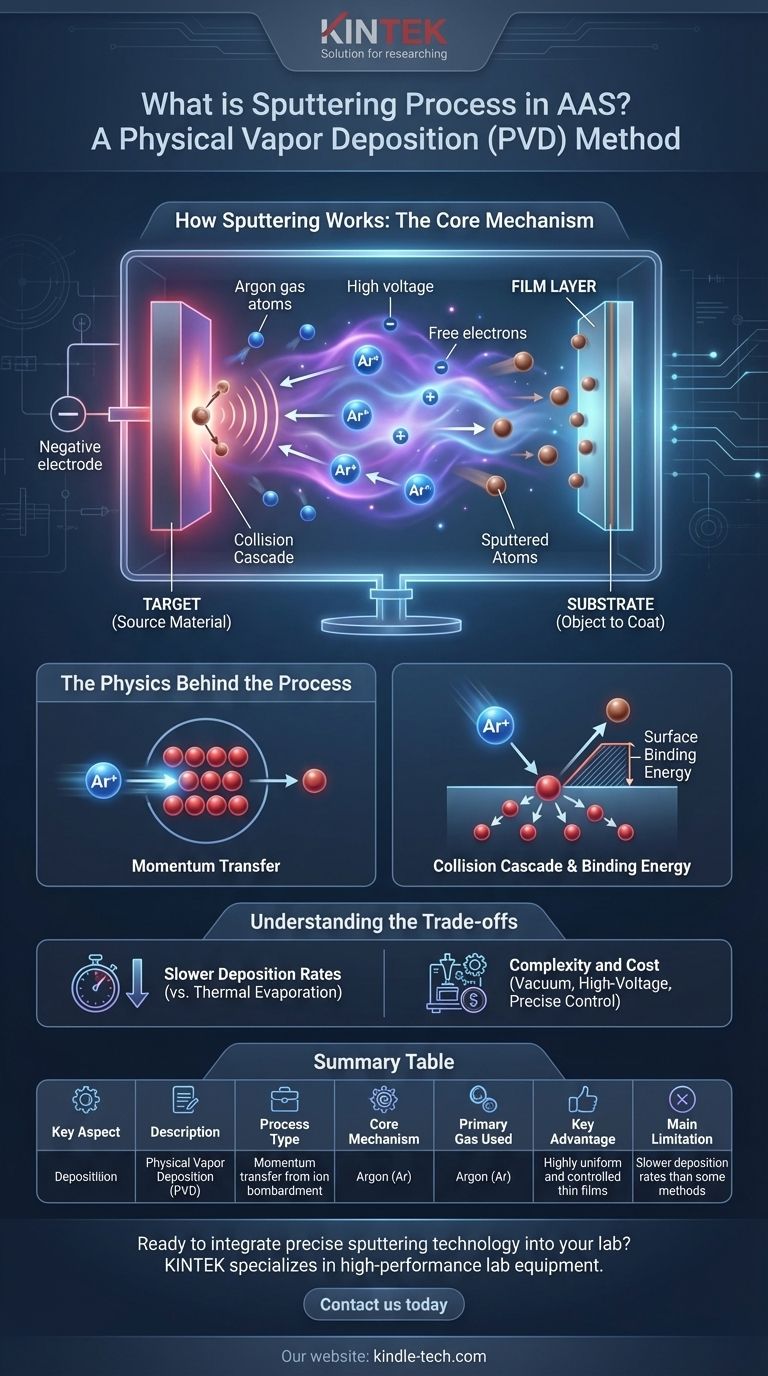
How Sputtering Works: The Core Mechanism
To understand sputtering, it's best to visualize it as a sequence of events occurring within a highly controlled environment.
The Essential Setup
The process begins by placing two key components into a vacuum chamber: the target and the substrate. The target is made of the material you wish to deposit, while the substrate is the object you want to coat.
The chamber is pumped down to a vacuum to remove contaminants. Then, a small, precise amount of an inert gas, almost always Argon (Ar), is introduced.
Creating the Plasma
A high voltage is applied across the chamber, making the target the negative electrode (cathode). This strong electric field energizes the inert gas.
Free electrons in the chamber accelerate and collide with the neutral Argon atoms, knocking off their electrons. This creates positively charged Argon ions (Ar+) and releases more electrons, resulting in a self-sustaining, glowing discharge known as a plasma.
The Bombardment Phase
The positively charged Argon ions are powerfully attracted and accelerated towards the negatively charged target.
They strike the target surface with tremendous kinetic energy. This is not a chemical reaction but a purely physical, high-impact collision.
Ejection and Deposition
The impact of the Argon ions dislodges or "sputters" atoms from the target material, ejecting them into the vacuum chamber.
These ejected atoms travel through the chamber and land on the substrate, condensing to form a thin, solid film. This process is repeated billions of time to build the film layer by atomic layer.
The Physics Behind the Process
Sputtering relies on fundamental principles of physics to achieve its precision. Understanding these concepts reveals why it is such a powerful technique.
It's All About Momentum Transfer
The core of the process is the transfer of momentum from the incoming Argon ion to the atoms of the target. It's a physical collision, similar to a cue ball striking a rack of billiard balls.
The efficiency of this transfer depends on the energy of the ions and the relative masses of the ion and target atoms.
Understanding the Collision Cascade
A single ion impact doesn't just chip off one atom. It sets off a collision cascade within the first few atomic layers of the target material.
Energy is transferred from atom to atom below the surface until the cascade reaches the surface with enough energy to eject an atom.
The Role of Surface Binding Energy
For a target atom to be sputtered, the energy it receives from the collision cascade must be greater than the surface binding energy. This is the energy that holds the atom to the bulk material.
This principle is why sputtering is a controlled physical process rather than a simple melting or evaporation technique.
Understanding the Trade-offs
While powerful, sputtering is not the ideal solution for every application. Its primary limitations are practical and economic.
Slower Deposition Rates
Compared to some other methods like thermal evaporation, sputtering can be a slower process. Building up thicker films can take a significant amount of time.
Complexity and Cost
Sputtering systems require a vacuum, high-voltage power supplies, and precise gas control. This makes the equipment complex and more expensive than simpler coating methods, representing a significant capital investment.
Applying This to Your Goal
Understanding sputtering allows you to appreciate its role in creating the high-performance materials that drive modern technology.
- If your primary focus is materials science: Recognize sputtering as a tool for creating films with precisely controlled grain structure, density, and orientation.
- If your primary focus is engineering or manufacturing: View sputtering as a highly reliable and repeatable process for producing uniform, durable, and functional coatings on components like semiconductors, optical lenses, and medical implants.
- If you are new to the topic: Remember the core concept: using high-energy ions in a plasma to physically knock atoms off a source and onto a surface.
Sputtering is a cornerstone technology, enabling the creation of materials and devices that would otherwise be impossible to fabricate.
Summary Table:
| Key Aspect | Description |
|---|---|
| Process Type | Physical Vapor Deposition (PVD) |
| Core Mechanism | Momentum transfer from ion bombardment |
| Primary Gas Used | Argon (Ar) |
| Key Advantage | Highly uniform and controlled thin films |
| Main Limitation | Slower deposition rates than some methods |
Ready to integrate precise sputtering technology into your lab? KINTEK specializes in high-performance lab equipment, including sputtering systems, to help you achieve superior thin-film coatings for your research and production needs. Our experts are ready to help you select the perfect solution. Contact us today to discuss your specific application!
Visual Guide
Related Products
- Spark Plasma Sintering Furnace SPS Furnace
- Vacuum Induction Melting Spinning System Arc Melting Furnace
- Chemical Vapor Deposition CVD Equipment System Chamber Slide PECVD Tube Furnace with Liquid Gasifier PECVD Machine
- Customer Made Versatile CVD Tube Furnace Chemical Vapor Deposition Chamber System Equipment
- HFCVD Machine System Equipment for Drawing Die Nano-Diamond Coating
People Also Ask
- What is the difference between spark plasma sintering and flash sintering? A Guide to Advanced Sintering Methods
- What are the fundamentals of spark plasma sintering process? Unlock Rapid, High-Performance Material Consolidation
- What is the mechanism of SPS process? A Deep Dive into Rapid, Low-Temperature Sintering
- What is the pressure for spark plasma sintering? A Guide to Optimizing SPS Parameters
- What technical advantages does a Spark Plasma Sintering (SPS) furnace offer for LZP ceramics? Enhance Ionic Conductivity


