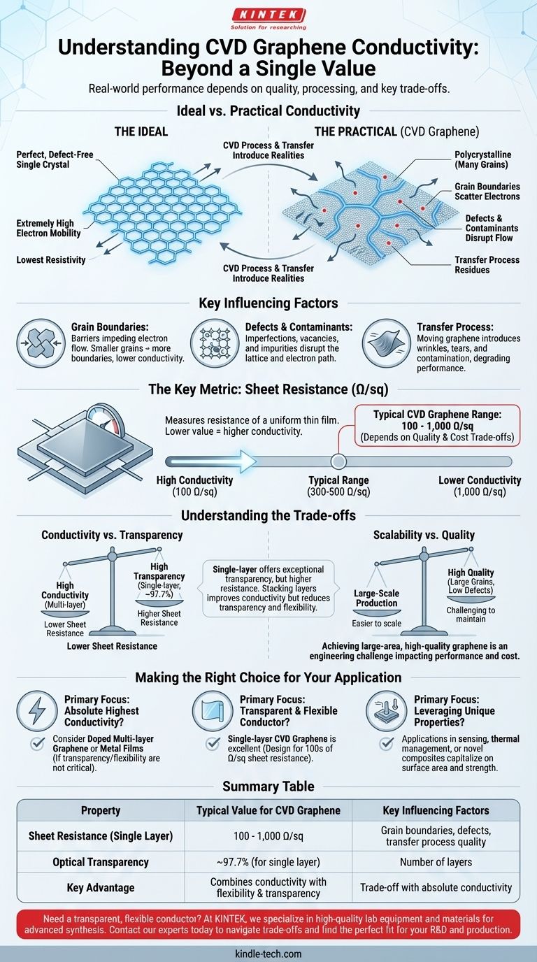
The electrical conductivity of CVD graphene is not a single, fixed value but a range determined by its quality and processing. While theoretically the most conductive material known, the practical conductivity of graphene produced via Chemical Vapor Deposition (CVD) is influenced by factors like grain boundaries, defects, and the transfer process. Its performance is most accurately measured by sheet resistance, which typically falls between 100 and 1,000 Ohms per square (Ω/sq) for a single layer.
The core issue is not simply the conductivity of CVD graphene, but understanding the trade-off between its excellent transparency and flexibility versus a conductivity that is good, but often lower than traditional materials like Indium Tin Oxide (ITO). Its true value lies in applications where this combination of properties is essential.
Why Real-World Conductivity Varies
Graphene's reputation as a "super-material" comes from the properties of a perfect, suspended, single-crystal flake. CVD graphene, designed for large-area production, introduces practical realities that modify these ideal properties.
The Ideal vs. The Practical
Theoretically, defect-free graphene has exceptionally high electron mobility, leading to extremely low resistivity. This is the source of its fame as the world's most conductive material.
However, CVD graphene is polycrystalline, meaning it is composed of many small, single-crystal "grains" that are stitched together during the growth process.
The Impact of Grain Boundaries
The boundaries between these crystal grains act as barriers that scatter electrons, impeding their flow. The smaller the grains, the more boundaries there are, and the lower the overall conductivity of the film.
Achieving large, single-crystal grains over a large area is a primary goal of advanced CVD research, as it directly improves electrical performance.
Defects and Contaminants
Any imperfection in the honeycomb lattice, such as missing atoms (vacancies) or impurities from the chemical process, can disrupt electron flow.
Furthermore, residues from the crucial step of transferring the graphene film from its growth substrate (typically copper) to a target substrate (like glass or plastic) are a major source of degraded conductivity.
Understanding the Key Metric: Sheet Resistance
For a two-dimensional material like graphene, a more practical measure than bulk conductivity is sheet resistance.
What is Sheet Resistance?
Sheet resistance, measured in Ohms per square (Ω/sq), describes the electrical resistance of a thin film of a uniform thickness. It is the standard metric used in industries that produce or use transparent conductive films.
A lower sheet resistance value indicates higher conductivity.
Typical Values for CVD Graphene
High-quality, research-grade single-layer CVD graphene can achieve a sheet resistance of around 100-300 Ω/sq.
More common, commercially produced large-area films may have a higher sheet resistance, often in the range of 400-1,000 Ω/sq, depending on the quality and cost trade-offs.
Understanding the Trade-offs
Choosing CVD graphene requires balancing its unique advantages against its practical limitations. It is not a universal replacement for all conductive materials.
The Critical Transfer Process
The process of moving the one-atom-thick graphene film from its copper growth foil to a final substrate is a significant challenge. This delicate step can introduce wrinkles, tears, and contamination, all of which negatively impact the final conductivity.
Conductivity vs. Transparency
Single-layer graphene offers exceptional optical transparency (absorbing only ~2.3% of visible light), but has the highest resistance.
Stacking multiple layers of graphene will decrease the sheet resistance (improve conductivity) but at the direct cost of reduced transparency and potentially lower flexibility.
Scalability vs. Quality
While CVD is hailed as the most promising method for large-scale production, there is often a trade-off between the size of the graphene sheet and its quality. Maintaining very low defect densities and large grain sizes over meter-scale production runs is a significant engineering challenge that impacts final performance and cost.
Making the Right Choice for Your Application
To decide if CVD graphene is the right material, you must evaluate its performance in the context of your specific requirements.
- If your primary focus is the absolute highest conductivity: Doped multi-layer graphene or traditional thin metal films may be more suitable, especially if transparency and flexibility are not critical.
- If your primary focus is a transparent and flexible conductor: Single-layer CVD graphene is an outstanding candidate, but you must design your device to function with a sheet resistance in the hundreds of Ω/sq.
- If your primary focus is leveraging its unique properties: Applications in sensing, thermal management, or creating novel composite materials can capitalize on graphene's large surface area and mechanical strength, where conductivity is a secondary, albeit useful, feature.
Ultimately, you must evaluate CVD graphene based on its unique balance of properties, not on a single, idealized metric.
Summary Table:
| Property | Typical Value for CVD Graphene | Key Influencing Factors |
|---|---|---|
| Sheet Resistance (Single Layer) | 100 - 1,000 Ω/sq | Grain boundaries, defects, transfer process quality |
| Optical Transparency | ~97.7% (for single layer) | Number of layers |
| Key Advantage | Combines conductivity with flexibility & transparency | Trade-off with absolute conductivity |
Need a transparent, flexible conductor for your next-generation device?
At KINTEK, we specialize in providing high-quality lab equipment and materials, including solutions for advanced material synthesis and characterization. Our expertise can help you navigate the trade-offs of materials like CVD graphene to find the perfect fit for your specific application—whether it's for flexible electronics, sensors, or composite materials.
Contact our experts today to discuss how we can support your R&D and production goals with reliable equipment and consumables tailored to your laboratory's needs.
Visual Guide
Related Products
- Laboratory CVD Boron Doped Diamond Materials
- CVD Diamond Wire Drawing Die Blanks for Precision Applications
- CVD Diamond for Thermal Management Applications
- CVD Diamond Dressing Tools for Precision Applications
- Custom CVD Diamond Coating for Lab Applications
People Also Ask
- What is the purpose of adding a boron source in CVD diamond growth? Master P-Type Semiconductor Conductivity
- What are the applications of CVD diamonds? From Jewelry to High-Tech Tools
- Do CVD diamonds pass diamond tester? Yes, they are real diamonds.
- What materials are CVD deposition? From Semiconductors to Super-Hard Coatings
- How much cheaper are CVD diamonds? Save 20-30% on a Genuine Diamond


