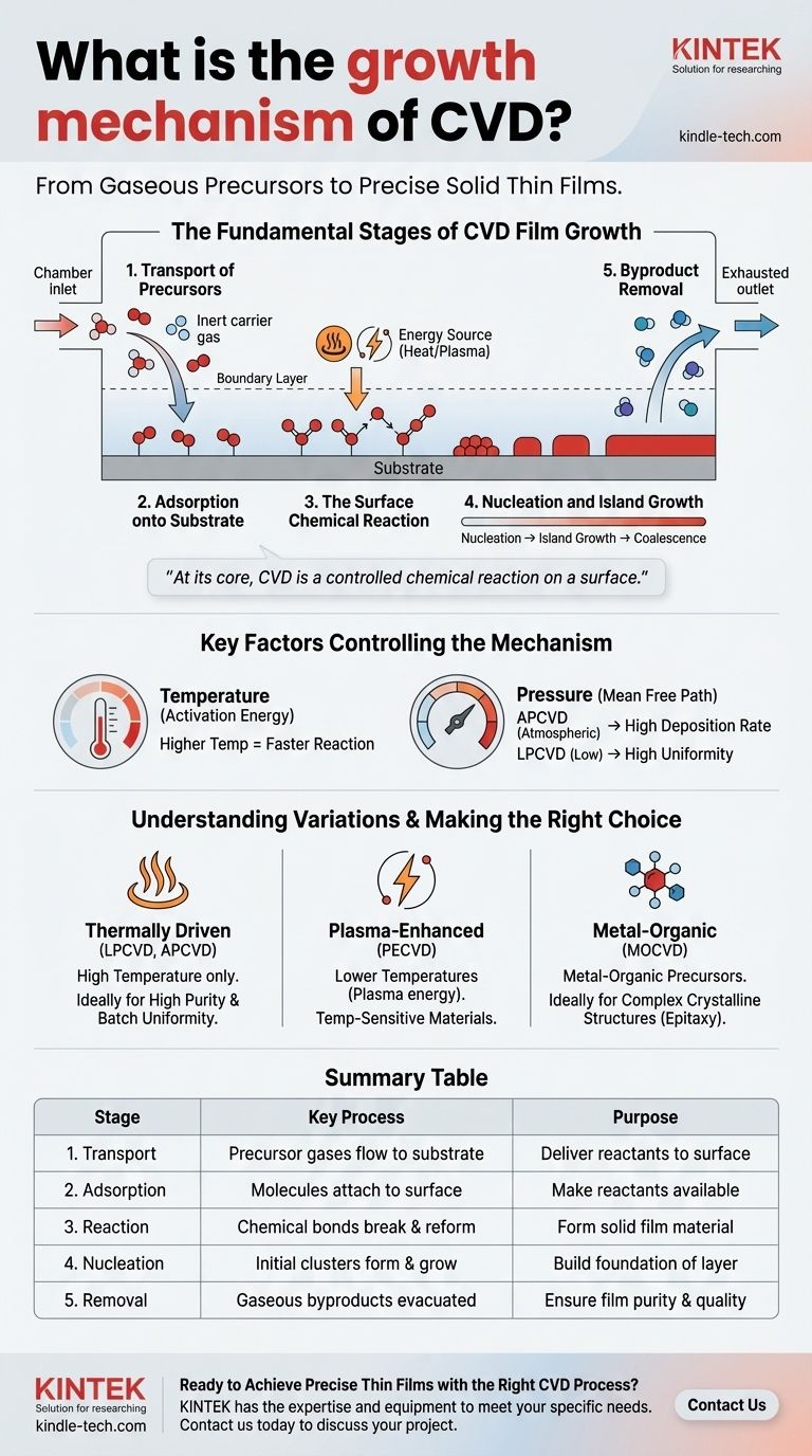
The fundamental growth mechanism of Chemical Vapor Deposition (CVD) is a multi-step process where gaseous chemical precursors are transported to a substrate, adsorb onto its surface, and then undergo a chemical reaction to form a solid thin film. The process begins with the introduction of reactant gases into a chamber, followed by their even distribution across the substrate (wafer). These precursors are absorbed, react to form initial "islands" of material that grow and merge, and finally, gaseous byproducts of the reaction are removed from the chamber.
At its core, CVD is a controlled chemical reaction on a surface. It transforms gas-phase molecules into a solid-state material, building a high-purity film layer by layer through a precise sequence of transport, adsorption, reaction, and removal.
The Fundamental Stages of CVD Film Growth
To truly understand CVD, you must see it as a sequence of distinct physical and chemical events. Each stage must be precisely controlled to achieve a high-quality, uniform film.
Stage 1: Transport of Precursors
The process begins with the introduction of one or more reactant gases, known as precursors, into the CVD reactor. These gases are carried toward the substrate, often by an inert carrier gas. A critical concept here is the boundary layer, a thin layer of stagnant gas just above the substrate surface, which the precursors must diffuse across to reach their destination.
Stage 2: Adsorption onto the Substrate
Once the precursor molecules reach the substrate, they must physically attach to the surface in a process called adsorption. This step is a prerequisite for any chemical reaction. The substrate holds the reactant molecules in place, making them available for the subsequent reaction stage.
Stage 3: The Surface Chemical Reaction
This is the heart of the CVD process. With thermal energy (heat) or another energy source like plasma, the adsorbed precursor molecules break their original chemical bonds and react. They form new, more stable bonds, creating the solid material that constitutes the desired film.
Stage 4: Nucleation and Island Growth
The film does not form instantaneously as a complete layer. The newly formed solid material first appears as tiny, isolated clusters called nuclei. These nuclei act as seeds, growing into larger "islands" as more reactions occur. Over time, these islands expand and merge together, a process called coalescence, to form a continuous, solid film across the entire substrate.
Stage 5: Byproduct Removal
The chemical reactions that form the solid film also create unwanted gaseous byproducts. These waste products must be efficiently desorbed from the surface and transported out of the reactor. Incomplete removal can lead to impurities being incorporated into the film, degrading its quality.
Key Factors Controlling the Growth Mechanism
The success of the CVD process hinges on controlling the variables that influence these stages. Temperature and pressure are the two most critical levers for manipulating the outcome.
The Role of Temperature
Temperature provides the activation energy needed for the chemical reactions on the substrate surface. Higher temperatures generally increase the reaction rate, but too much heat can cause unwanted gas-phase reactions before the precursors even reach the substrate.
The Impact of Pressure
Pressure dictates the concentration and mean free path of the gas molecules.
- Atmospheric Pressure (APCVD) results in a very thin boundary layer, leading to high deposition rates.
- Low Pressure (LPCVD) increases the mean free path of gas molecules, allowing for more uniform coating of many substrates at once, even on complex surfaces.
Understanding Variations in the Mechanism
While the five fundamental stages remain consistent, different types of CVD use different methods to drive the surface reaction.
Thermally Driven CVD (LPCVD, APCVD)
This is the classic mechanism where high temperature is the sole energy source used to initiate the chemical reaction on the heated substrate.
Plasma-Enhanced CVD (PECVD)
PECVD uses an electric field to generate a plasma, an energized gas. This plasma provides the energy to break precursor bonds, allowing the chemical reaction to occur at much lower temperatures. This is critical for depositing films on substrates that cannot withstand high heat.
Metal-Organic CVD (MOCVD)
MOCVD is a specialized form of CVD that uses metal-organic compounds as precursors. This technique offers exceptionally fine control over the film's composition, making it essential for manufacturing complex semiconductor devices like LEDs and high-power electronics.
Making the Right Choice for Your Goal
Selecting the correct CVD method requires matching the process characteristics to the desired outcome for the film.
- If your primary focus is high purity and batch uniformity: LPCVD is often chosen because the reduced pressure enables excellent precursor distribution across many wafers.
- If your primary focus is depositing on temperature-sensitive materials: PECVD is the ideal choice because the plasma provides the reaction energy, allowing for significantly lower process temperatures.
- If your primary focus is creating complex crystalline structures (epitaxy): MOCVD provides the precise chemical control necessary to build these advanced material layers.
Ultimately, understanding these fundamental growth stages allows you to select and control the right CVD process to achieve the desired film properties for any application.
Summary Table:
| Stage | Key Process | Purpose |
|---|---|---|
| 1. Transport | Precursor gases flow to the substrate | Deliver reactants to the surface |
| 2. Adsorption | Molecules attach to the substrate surface | Make reactants available for reaction |
| 3. Reaction | Chemical bonds break and reform (aided by heat/plasma) | Form the solid film material |
| 4. Nucleation | Initial clusters (nuclei) form and grow into a continuous film | Build the foundation of the layer |
| 5. Removal | Gaseous byproducts are desorbed and evacuated | Ensure film purity and quality |
Ready to Achieve Precise Thin Films with the Right CVD Process?
Understanding the growth mechanism is the first step to optimizing your deposition. Whether you require the high uniformity of LPCVD, the low-temperature capabilities of PECVD, or the precise compositional control of MOCVD, KINTEK has the expertise and equipment to meet your laboratory's specific needs.
Contact us today via our [#ContactForm] to discuss your project. Let our specialists help you select the ideal CVD solution to enhance your research and development outcomes.
Visual Guide
Related Products
- Microwave Plasma Chemical Vapor Deposition MPCVD Machine System Reactor for Lab and Diamond Growth
- Cylindrical Resonator MPCVD Machine System Reactor for Microwave Plasma Chemical Vapor Deposition and Lab Diamond Growth
- 915MHz MPCVD Diamond Machine Microwave Plasma Chemical Vapor Deposition System Reactor
- Chemical Vapor Deposition CVD Equipment System Chamber Slide PECVD Tube Furnace with Liquid Gasifier PECVD Machine
- Custom CVD Diamond Coating for Lab Applications
People Also Ask
- How does MPCVD work? A Guide to Low-Temperature, High-Quality Film Deposition
- What pressure is needed for chemical vapor deposition of diamonds? Master the Low-Pressure 'Sweet Spot'
- What are the advantages of a Microwave Plasma CVD reactor for MCD/NCD coatings? Precision Multilayer Diamond Engineering
- How do vacuum pumps and valves collaborate in MPCVD? Achieve Precise Pressure Control for Superior CNT Synthesis
- What is microwave plasma chemical vapor deposition? A Guide to High-Purity Diamond Film Growth


