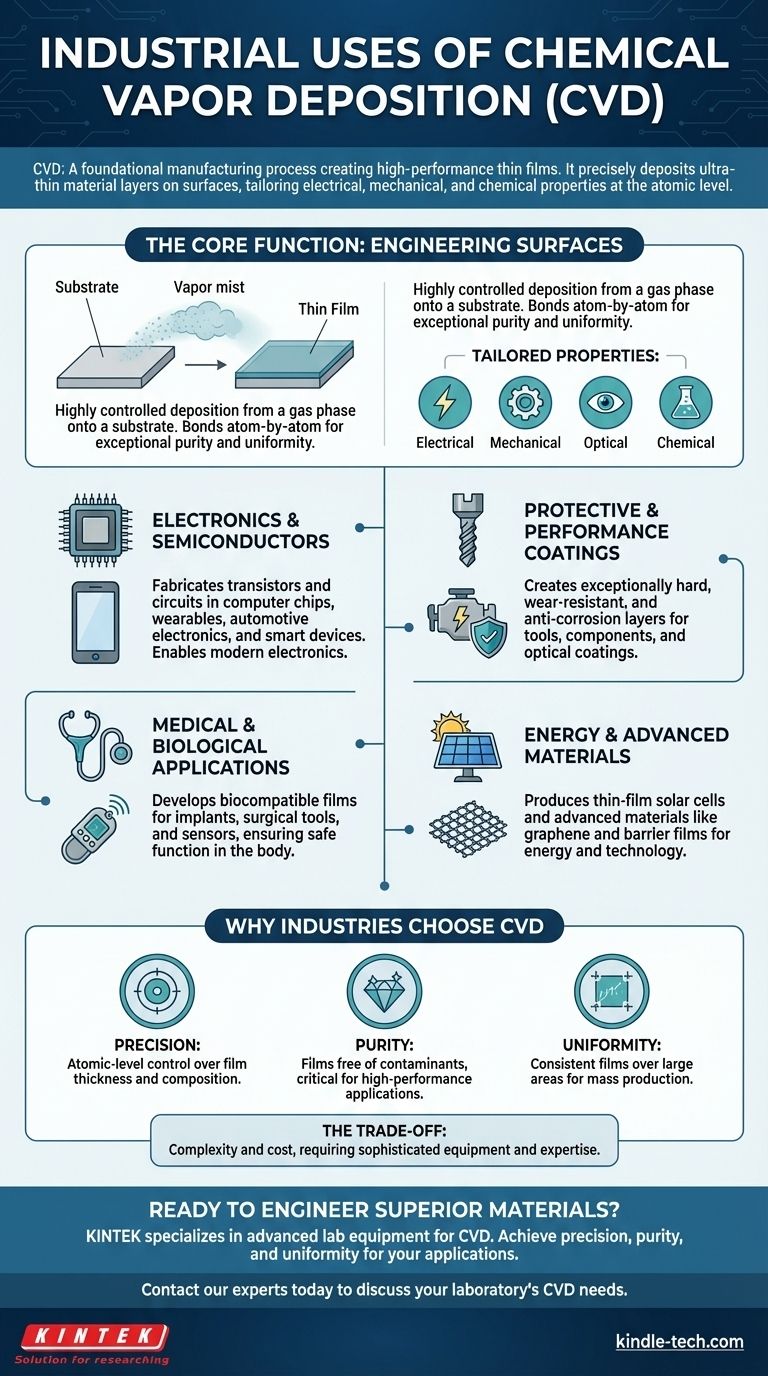
In short, Chemical Vapor Deposition (CVD) is a foundational manufacturing process used across a vast range of industries to create high-performance thin films. Its primary industrial applications are in fabricating semiconductor devices for electronics, applying hard and corrosion-resistant protective coatings on tools and parts, and developing advanced materials for the medical and energy sectors.
At its core, CVD is not about a single product but about a capability: the precise control to deposit ultra-thin layers of material onto a surface. This ability to fundamentally engineer the properties of an object—making it stronger, more conductive, or biocompatible—is why CVD is indispensable to modern technology.
The Core Function: Engineering Surfaces at the Atomic Level
What is Chemical Vapor Deposition?
Chemical Vapor Deposition (CVD) is a process where a solid material is deposited from a gaseous phase onto a substrate. Think of it as a highly controlled "spray painting" process that happens at a molecular level inside a reaction chamber.
The result is an exceptionally thin, pure, and uniform layer, or thin film, that bonds to the underlying surface. This film imparts new properties to the original object.
The Goal: Tailoring Material Properties
Industries don't use CVD just to add a layer; they use it to fundamentally change an object's performance. The goal is to give a material specific electrical, mechanical, optical, or chemical properties it doesn't naturally possess.
This precision is the key to its widespread industrial adoption.
Key Industrial Application Domains
Electronics and Semiconductors
This is the largest and most critical application of CVD. Modern electronics would not exist without it.
CVD is used to deposit the multiple layers of conductive, insulating, and semiconducting materials that form the microscopic transistors and circuits inside computer chips. This applies to everything from smartphones and wearables to automotive electronics and smart home devices.
Protective and Performance Coatings
CVD is used to create exceptionally hard and durable coatings that protect tools and components from wear and corrosion.
Cutting tools, drill bits, and industrial engine parts are often coated using CVD to dramatically extend their lifespan and improve performance. On a more common level, CVD can be used to apply the scratch-resistant and anti-reflective coatings on sunglasses.
Medical and Biological Applications
The process can create biocompatible films that the human body will not reject.
These coatings are critical for medical implants, surgical tools, and biosensors, ensuring they can function safely and effectively within a biological environment.
Energy and Advanced Materials
CVD is essential for producing next-generation energy and material technologies. It is a key step in fabricating thin-film solar cells.
Researchers also use CVD to produce advanced materials like large-scale sheets of graphene. Even everyday items like potato chip bags use a thin, metalized film created through a similar process to act as a barrier to oxygen and moisture.
Understanding the Value Proposition
Why Industries Choose CVD
The industrial value of CVD comes down to three factors: precision, purity, and uniformity. The process allows for atomic-level control over film thickness and composition.
Because the deposition happens from a highly pure gas, the resulting films are free of contaminants. This is absolutely critical in semiconductor manufacturing, where a single microscopic impurity can ruin a chip.
Finally, CVD can apply these perfect films uniformly over large areas, such as an entire silicon wafer containing hundreds of chips, making it suitable for mass production.
The Trade-off: Complexity and Cost
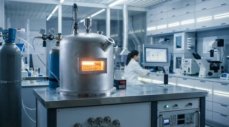
CVD is not a simple process. It requires sophisticated equipment, including vacuum chambers, high-temperature furnaces, and systems for handling precursor gases.
This represents a significant capital investment and requires specialized expertise to operate. Therefore, it is typically reserved for applications where the high performance it enables justifies the cost.
Making the Right Choice for Your Goal
The decision to use CVD is driven entirely by the performance requirements of the final product.
- If your primary focus is mass-market electronics: CVD is the non-negotiable standard for fabricating the core semiconductor components that power your devices.
- If your primary focus is mechanical durability: CVD provides superior wear-resistant and anti-corrosion coatings for high-performance tools and industrial components.
- If your primary focus is biomedical compatibility: CVD is the go-to method for creating the inert, biocompatible surfaces required for medical implants and sensors.
- If your primary focus is next-generation technology: CVD is an indispensable research and production tool for creating novel materials for the energy and advanced materials sectors.
Ultimately, mastering CVD means mastering the ability to engineer material properties on demand for nearly any high-value application.
Summary Table:
| Application Domain | Key Uses of CVD |
|---|---|
| Electronics & Semiconductors | Fabricating transistors and circuits in computer chips, smartphones, and automotive electronics. |
| Protective Coatings | Applying hard, wear-resistant layers on cutting tools, drill bits, and engine parts. |
| Medical & Biological | Creating biocompatible films for surgical implants, tools, and biosensors. |
| Energy & Advanced Materials | Producing thin-film solar cells and advanced materials like graphene. |
Ready to engineer superior material properties for your application?
KINTEK specializes in providing advanced lab equipment and consumables for Chemical Vapor Deposition processes. Whether you are developing next-generation semiconductors, durable protective coatings, or biocompatible medical devices, our solutions deliver the precision, purity, and uniformity required for high-performance results.
Contact our experts today to discuss how KINTEK can support your laboratory's CVD needs and help you achieve your material engineering goals.
Visual Guide
Related Products
- CVD Diamond Dressing Tools for Precision Applications
- Multi Heating Zones CVD Tube Furnace Machine Chemical Vapor Deposition Chamber System Equipment
- CVD Diamond Domes for Industrial and Scientific Applications
- CVD Diamond for Thermal Management Applications
- Chemical Vapor Deposition CVD Equipment System Chamber Slide PECVD Tube Furnace with Liquid Gasifier PECVD Machine
People Also Ask
- What is chemical vapor deposition of diamond? Grow High-Purity Diamonds Atom-by-Atom
- What color diamonds are CVD? Understanding the Process from Brown Tint to Colorless Beauty
- How do CVD diamonds grow? A Step-by-Step Guide to Lab-Grown Diamond Creation
- Does the chemical vapor deposition be used for diamonds? Yes, for Growing High-Purity Lab Diamonds
- Can CVD diamonds change color? No, their color is permanent and stable.


