In essence, Metal-Organic Chemical Vapor Deposition (MOCVD) is a highly precise industrial process used to grow ultra-thin, perfect crystalline films on a substrate. It functions by introducing specific metal-organic precursor gases into a reaction chamber, where they chemically react on a heated surface to deposit material one atomic layer at a time. This technique is the backbone of manufacturing for many high-performance semiconductor devices.
At its core, building modern electronics requires creating flawless crystal structures on an industrial scale. MOCVD solves this challenge by using controlled chemical reactions in a vapor phase, making it the dominant technology for producing the high-purity compound semiconductors that power devices like LEDs and lasers.
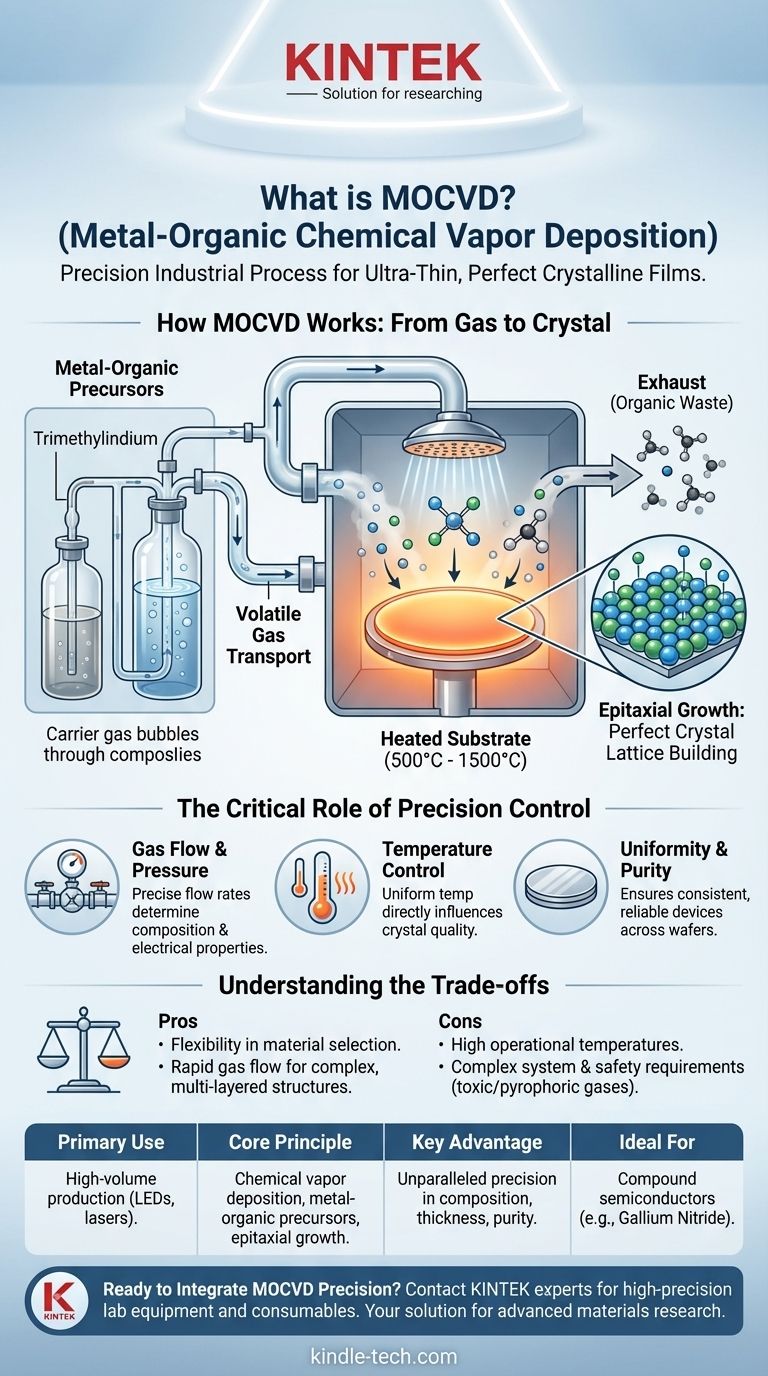
How MOCVD Works: From Gas to Crystal
MOCVD is a sophisticated process that transforms volatile chemical compounds into solid, highly ordered crystalline layers. Understanding its mechanism reveals why it is so powerful for fabricating advanced materials.
The Core Principle: Chemical Vapor Deposition
The fundamental idea is to transport material to a surface in gas form. Once the gas molecules reach the heated substrate, they undergo a chemical reaction and deposit as a thin solid film.
The "Metal-Organic" Precursors
MOCVD uses special source materials called metal-organics (e.g., trimethylindium). These compounds contain the desired metal atom (like indium) bonded to organic molecules, which makes them volatile at manageable temperatures.
These precursors are typically held in containers called bubblers. A precisely controlled carrier gas is bubbled through the liquid precursor, picking up a known concentration of its vapor and carrying it toward the reaction chamber.
The Reaction Chamber and Substrate
Inside the chamber, a substrate wafer is heated to a high temperature, often between 500°C and 1500°C. When the precursor gases flow over this hot surface, the heat provides the energy needed to break their chemical bonds.
This reaction deposits the desired metal atoms (like gallium or indium) onto the substrate, while the leftover organic components are flushed out as exhaust gas.
Epitaxial Growth: Building the Perfect Lattice
The result of this process is epitaxial growth. This means the deposited atoms arrange themselves to mirror the underlying crystal structure of the substrate, creating a seamless, single-crystal film with exceptionally high purity and few defects. This perfection is critical for the electrical and optical properties of the final device.
The Critical Role of Precision Control
The defining advantage of MOCVD is its ability to be controlled with extreme precision. Every variable is monitored and managed to ensure a repeatable, high-yield manufacturing process.
Managing Gas Flow and Pressure
The MOCVD system features a complex gas transportation network. By precisely controlling the flow rates of different precursor and dopant gases, manufacturers can accurately determine the final film's chemical composition and electrical properties. Fast-acting valves allow for the creation of abrupt, atomically sharp interfaces between different material layers.
The Importance of Temperature
Temperature control is paramount. The substrate's temperature dictates the rate of the chemical reaction and directly influences the quality of the resulting crystal. A single, uniform temperature across the wafer ensures the material grown is homogeneous.
Achieving Uniformity and Purity
The combination of precise control over gas flow, pressure, and temperature allows MOCVD to produce films with outstanding thickness uniformity and purity across large wafers. This is essential for mass-producing reliable electronic devices.
Understanding the Trade-offs
While powerful, MOCVD is a complex technology with specific operational considerations. Understanding its trade-offs is key to appreciating its role.
High Operational Temperatures
The high temperatures required for the chemical reactions are ideal for robust materials like gallium nitride (GaN) but can be a limitation for materials that are not stable at such heat. This makes MOCVD highly specialized for certain classes of semiconductors.
System Complexity and Safety
An MOCVD system is a sophisticated piece of machinery with multiple integrated subsystems for gas delivery, temperature control, and exhaust treatment. Furthermore, the metal-organic precursors and other gases used are often toxic or pyrophoric (igniting on contact with air), demanding robust safety and alarm systems.
Flexibility and Speed
The technology offers incredible flexibility in material selection. The fast gas flow rates allow for rapid changes in composition, enabling the growth of complex, multi-layered device structures. This speed in changing layers is a key advantage over some alternative methods.
Making the Right Choice for Your Goal
MOCVD is a cornerstone of semiconductor fabrication, but its application depends on the desired outcome.
- If your primary focus is high-volume production of LEDs or semiconductor lasers: MOCVD is the undisputed industry standard, offering the scalability, precision, and yield required for mass manufacturing.
- If your primary focus is growing high-quality compound semiconductors like GaN: MOCVD is the superior choice due to its effectiveness in handling the necessary precursor chemistry and high growth temperatures.
- If your primary focus is ensuring reproducible device performance: The unparalleled process control of MOCVD ensures that films grown today are identical to films grown months from now, guaranteeing consistent yields.
Ultimately, MOCVD's ability to precisely construct materials atom by atom is what enables the fabrication of the high-performance electronic and photonic devices that define our modern world.
Summary Table:
| Key Aspect | Description |
|---|---|
| Primary Use | High-volume production of compound semiconductor devices (e.g., LEDs, lasers). |
| Core Principle | Chemical vapor deposition using metal-organic precursors for epitaxial growth. |
| Key Advantage | Unparalleled precision in controlling film composition, thickness, and purity. |
| Ideal For | Manufacturing materials like Gallium Nitride (GaN) that require high growth temperatures. |
Ready to Integrate MOCVD Precision into Your Lab?
MOCVD is the cornerstone of advanced semiconductor fabrication, enabling the production of devices with exceptional performance and reliability. KINTEK specializes in providing the high-precision lab equipment and consumables necessary for cutting-edge materials research and development.
Whether you are scaling up production or pushing the boundaries of compound semiconductor growth, our expertise can help you achieve the uniformity and yield your projects demand.
Contact our experts today to discuss how our solutions can power your next breakthrough.
Visual Guide
Related Products
- Microwave Plasma Chemical Vapor Deposition MPCVD Machine System Reactor for Lab and Diamond Growth
- Multi Heating Zones CVD Tube Furnace Machine Chemical Vapor Deposition Chamber System Equipment
- 915MHz MPCVD Diamond Machine Microwave Plasma Chemical Vapor Deposition System Reactor
- Cylindrical Resonator MPCVD Machine System Reactor for Microwave Plasma Chemical Vapor Deposition and Lab Diamond Growth
- Chemical Vapor Deposition CVD Equipment System Chamber Slide PECVD Tube Furnace with Liquid Gasifier PECVD Machine
People Also Ask
- How do vacuum pumps and valves collaborate in MPCVD? Achieve Precise Pressure Control for Superior CNT Synthesis
- How is a diamond formed from CVD? The Science of Growing Diamonds Atom by Atom
- How does a microwave plasma reactor facilitate the synthesis of diamond? Master MPCVD with Precision Technology
- How does MPCVD work? A Guide to Low-Temperature, High-Quality Film Deposition
- How are CVD diamonds created? Discover the Science of Lab-Grown Diamond Precision


