At its core, Metal-Organic Chemical Vapor Deposition (MOCVD) is a highly controlled manufacturing process used to grow high-purity, crystalline thin films on a substrate. It achieves this by introducing volatile metal-organic precursors and other gases into a reaction chamber, where they chemically react on a heated surface to form a solid layer. This technique is the cornerstone for producing many modern semiconductor devices, including LEDs.
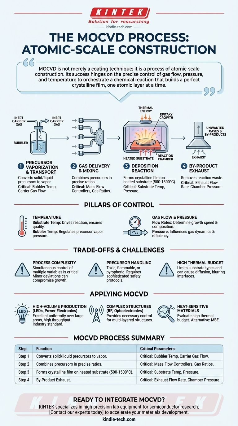
MOCVD is not merely a coating technique; it is a process of atomic-scale construction. Its success hinges on the precise control of gas flow, pressure, and temperature to orchestrate a chemical reaction that builds a perfect crystalline film, one atomic layer at a time.
How MOCVD Translates Gas into Solid Crystal
The MOCVD process can be understood as a four-step production line that transforms carefully selected gases into a solid, functional material.
Step 1: Precursor Vaporization and Transport
The process begins with the source materials, known as metal-organic (MO) precursors. These compounds contain the metal atoms needed for the final film.
These precursors are often liquids or solids held in a container called a bubbler. A precisely controlled stream of an inert carrier gas (like hydrogen or nitrogen) is bubbled through the precursor, carrying a specific concentration of its vapor out of the container.
Step 2: Gas Delivery and Mixing
The precursor-laden carrier gas then travels through dedicated gas lines. It is mixed with other reactive gases at the inlet of the main reaction chamber.
The ratio of these mixed gases is critical, as it will directly determine the chemical composition of the final crystalline film.
Step 3: The Deposition Reaction
The gas mixture flows over a heated substrate (often a semiconductor wafer) inside the reaction chamber. Substrate temperatures are typically very high, ranging from 500 to 1500°C.
This intense heat provides the energy for the precursor molecules to decompose and react on the substrate surface. This chemical reaction deposits the desired material as a thin, highly ordered crystalline film. This type of growth, where the crystal structure of the film mimics the substrate, is known as epitaxy.
Step 4: By-product Exhaust
The chemical reaction creates the solid film on the wafer, but it also produces unwanted gaseous by-products.
These by-products, along with any unreacted precursor gases, are continuously swept away by the gas flow and safely removed from the chamber.
The Pillars of Control in MOCVD
The quality, thickness, and composition of the film are not left to chance. They are dictated by three tightly controlled process variables.
The Role of Temperature
Temperature is the primary driver of the deposition reaction. The substrate temperature must be high enough to break the chemical bonds in the precursor molecules but optimized to ensure high-quality crystal growth. The bubbler temperature is also controlled independently to regulate the vapor pressure of the precursor, which determines its concentration in the gas stream.
The Importance of Gas Flow and Pressure
The flow rates of the carrier and reactive gases are managed by mass flow controllers. These rates determine the growth speed and the elemental makeup of the film. For example, in growing a compound semiconductor like Gallium Arsenide (GaAs), the ratio of the gallium precursor flow to the arsenic precursor flow is paramount.
The pressure inside the chamber is also a key variable, influencing gas flow dynamics and the efficiency of the chemical reactions on the surface.
Understanding the Trade-offs and Challenges
While powerful, MOCVD is a complex process with inherent challenges that must be managed for successful fabrication.
Process Complexity
The quality of the final product depends on the precise and simultaneous control of multiple variables: gas flows, temperatures, pressure, and even the geometry of the reactor. A minor deviation in any one of these can compromise the entire growth run.
Precursor Handling
Metal-organic precursors can be highly toxic, flammable, or pyrophoric (igniting spontaneously in air). This requires sophisticated safety protocols and handling systems, adding to the operational complexity and cost.
High Thermal Budget
The high temperatures required for deposition are a double-edged sword. While necessary for the reaction, they can limit the types of materials that can be used as substrates and can sometimes cause diffusion between different layers in a complex device structure, blurring sharp interfaces.
Applying MOCVD to Your Project
Your decision to use MOCVD should be based on the specific requirements of the material and device you intend to create.
- If your primary focus is high-volume production of devices like LEDs or power electronics: MOCVD is the established industry standard, offering excellent uniformity over large wafer areas and high throughput.
- If your primary focus is growing III-V compound semiconductors for RF or optoelectronics: MOCVD provides the control necessary to create the complex, multi-layered structures these devices require.
- If your primary focus is on materials sensitive to high heat or requiring atomically sharp interfaces: You must carefully evaluate if the high thermal budget of MOCVD is acceptable, or if an alternative like Molecular Beam Epitaxy (MBE) might be more suitable.
Ultimately, MOCVD is the workhorse technology that enables the mass production of the advanced semiconductor materials powering our modern world.
Summary Table:
| MOCVD Process Step | Key Function | Critical Parameters |
|---|---|---|
| 1. Precursor Vaporization | Converts solid/liquid precursors to vapor | Bubbler temperature, Carrier gas flow |
| 2. Gas Delivery & Mixing | Combines precursors in precise ratios | Mass flow controller settings, Gas ratios |
| 3. Deposition Reaction | Forms crystalline film on heated substrate | Substrate temperature (500-1500°C), Pressure |
| 4. By-product Exhaust | Removes reaction waste from chamber | Exhaust flow rate, Chamber pressure |
Ready to Integrate MOCVD into Your Lab Workflow?
KINTEK specializes in providing high-precision lab equipment and consumables for semiconductor research and production. Whether you are developing next-generation LEDs, power electronics, or compound semiconductors, our MOCVD solutions offer the precise temperature control, gas management, and safety features required for successful thin-film deposition.
Contact our experts today to discuss how our reliable MOCVD systems and support can accelerate your materials development and scale your production efficiently.
Visual Guide
Related Products
- Multi Heating Zones CVD Tube Furnace Machine Chemical Vapor Deposition Chamber System Equipment
- 915MHz MPCVD Diamond Machine Microwave Plasma Chemical Vapor Deposition System Reactor
- Microwave Plasma Chemical Vapor Deposition MPCVD Machine System Reactor for Lab and Diamond Growth
- Cylindrical Resonator MPCVD Machine System Reactor for Microwave Plasma Chemical Vapor Deposition and Lab Diamond Growth
- Molybdenum Vacuum Heat Treat Furnace
People Also Ask
- What are the advantages of a multi-zone tube furnace for Sb2S3? Unlock Superior Semiconductor Thin Film Purity
- What is a CVD tube furnace? A Complete Guide to Thin-Film Deposition
- What are the advantages of using a Multi-zone Tube Furnace? Enhanced Thermal Uniformity for Diffusion Research
- What are the differences between chemical vapour deposition processes? A Guide to Pressure, Quality & Cost
- What is the function of a tube furnace in CVD SiC synthesis? Achieving Ultra-Pure Silicon Carbide Powders