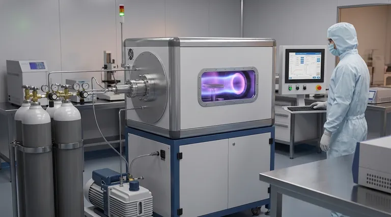
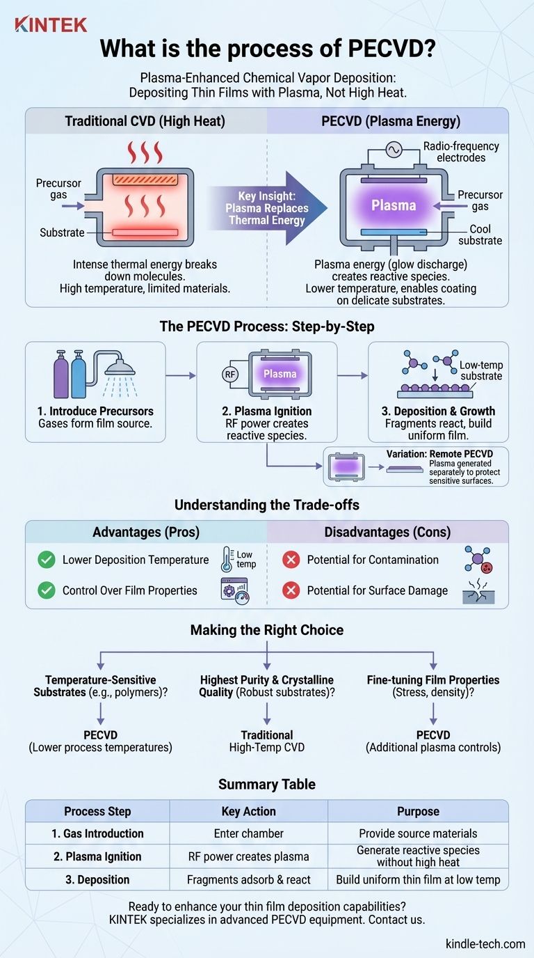
At its core, Plasma-Enhanced Chemical Vapor Deposition (PECVD) is a process used to deposit thin, solid films from a gas onto a substrate. Unlike traditional Chemical Vapor Deposition (CVD) which relies on intense heat to drive chemical reactions, PECVD uses the energy from a plasma to achieve the same result at much lower temperatures. This allows for the coating of materials that would otherwise be damaged by high-heat processes.
The crucial insight is that PECVD substitutes the thermal energy of conventional methods with plasma energy. This fundamental difference allows for the creation of high-quality thin films on temperature-sensitive substrates, dramatically expanding the range of possible applications in electronics, optics, and materials science.
The Core Principle: Replacing Heat with Plasma
To understand PECVD, it's essential to first distinguish it from its predecessor, traditional Chemical Vapor Deposition (CVD).
Distinguishing PECVD from Traditional CVD
Traditional CVD involves passing a volatile precursor gas over a substrate heated to a very high temperature (often several hundred degrees Celsius). This intense heat provides the energy needed to break down the precursor molecules, causing them to react and deposit a solid film onto the substrate surface.
The primary limitation of this method is the high temperature, which makes it unsuitable for coating plastics, polymers, or other delicate materials.
The Role of Plasma
PECVD overcomes this limitation by generating a plasma, an energized state of gas often called a "glow discharge." This is typically achieved by applying radio-frequency (RF) energy (e.g., at 13.56 MHz) across two electrodes within a low-pressure reaction chamber.
The plasma consists of a mixture of ions, electrons, and highly reactive neutral species (radicals).
Creating Reactive Species Through Energy
The high-energy electrons within the plasma collide with the precursor gas molecules. These collisions are energetic enough to fragment the precursor molecules into the reactive chemical species needed for deposition.
Essentially, the plasma's energy, not the substrate's heat, is the primary driver of the chemical reaction.
The Step-by-Step PECVD Process
While equipment specifics vary, the fundamental process follows a clear sequence of events inside a vacuum chamber.
1. Introducing Precursor Gases
Reactant gases, also known as precursors, are introduced into the process chamber. These are the source materials that will form the final film.
To ensure a uniform coating, the gases are often distributed over the substrate through a perforated plate known as a shower head.
2. Plasma Ignition
RF power is applied to the electrodes within the chamber, igniting the precursor gas mixture and sustaining it as a plasma. This glow discharge provides the energy for the next step.
3. Deposition and Film Growth
The reactive molecular fragments created in the plasma adsorb onto the substrate's surface. The substrate is typically heated, but to a much lower temperature than in CVD.
On the surface, these fragments react, bond, and build up over time to form a uniform, solid thin film.
Process Variation: Remote PECVD
In some applications, direct exposure to the plasma can damage a sensitive substrate. To mitigate this, a remote PECVD method can be used.
In this technique, the plasma is generated in a separate chamber. The reactive species are then extracted and transported to the substrate, which remains in a plasma-free region for deposition.
Understanding the Trade-offs
PECVD is a powerful technique, but its advantages come with specific considerations that must be weighed against other methods.
Advantage: Lower Deposition Temperature
This is the most significant benefit of PECVD. It enables the deposition of high-quality films on materials like plastics, flexible electronics, and other temperature-sensitive components without causing thermal damage.
Advantage: Control Over Film Properties
The use of plasma introduces additional process variables (e.g., RF power, pressure, gas flow rates) that are not available in traditional CVD. These parameters allow for fine-tuning of the final film's properties, such as its density, stress, and chemical composition.
Disadvantage: Potential for Contamination
The complex reactions occurring within the plasma can sometimes lead to the incorporation of unwanted elements, like hydrogen from precursor gases, into the final film. This can affect the film's purity and electrical characteristics compared to films grown via high-temperature CVD.
Disadvantage: Potential for Surface Damage
While far gentler than high heat, direct exposure to an energetic plasma can still cause some degree of surface damage or create defects on highly sensitive substrates. This is the primary reason for using advanced techniques like remote PECVD.
Making the Right Choice for Your Goal
Selecting the correct deposition method depends entirely on the requirements of your substrate and the desired properties of the final film.
- If your primary focus is depositing on temperature-sensitive substrates (like polymers): PECVD is the superior choice due to its significantly lower process temperatures.
- If your primary focus is achieving the highest possible film purity and crystalline quality for robust substrates: Traditional high-temperature CVD may be required, provided your substrate can withstand the heat.
- If your primary focus is fine-tuning film properties like mechanical stress and density: The additional control parameters offered by the plasma in PECVD provide a distinct advantage.
Ultimately, understanding the interplay between plasma energy and chemical reaction is key to leveraging PECVD to achieve results that are impossible with purely thermal methods.
Summary Table:
| Process Step | Key Action | Purpose |
|---|---|---|
| 1. Gas Introduction | Precursor gases enter chamber | Provide source materials for film formation |
| 2. Plasma Ignition | RF power creates plasma | Generate reactive species without high heat |
| 3. Deposition | Fragments adsorb and react on substrate | Build uniform thin film at low temperature |
| Key Advantage | Lower temperature process | Enables coating of delicate materials |
| Key Consideration | Potential plasma damage | May require remote PECVD for sensitive substrates |
Ready to enhance your thin film deposition capabilities?
KINTEK specializes in advanced lab equipment for PECVD applications, serving research and industrial laboratories worldwide. Our expertise in plasma-enhanced deposition technology can help you:
- Deposit high-quality thin films on temperature-sensitive substrates
- Achieve precise control over film properties and composition
- Optimize your deposition process for materials science, electronics, and optics applications
Let our team provide the right PECVD solution for your specific laboratory needs. Contact us today to discuss how we can support your thin film deposition goals!
Visual Guide
Related Products
- Inclined Rotary Plasma Enhanced Chemical Vapor Deposition PECVD Equipment Tube Furnace Machine
- Chemical Vapor Deposition CVD Equipment System Chamber Slide PECVD Tube Furnace with Liquid Gasifier PECVD Machine
- Inclined Rotary Plasma Enhanced Chemical Vapor Deposition PECVD Equipment Tube Furnace Machine
- RF PECVD System Radio Frequency Plasma-Enhanced Chemical Vapor Deposition RF PECVD
- Multi Heating Zones CVD Tube Furnace Machine Chemical Vapor Deposition Chamber System Equipment
People Also Ask
- How does PECVD equipment facilitate the directional growth of carbon nanotubes? Achieve Precision Vertical Alignment
- Why is a PECVD system required for vertical graphene synthesis? Master Directional Control for 3D Nanostructures
- What are the benefits of plasma enhanced CVD? Achieve High-Quality, Low-Temperature Film Deposition
- How does plasma enhanced chemical vapor deposition work? Enable Low-Temperature Thin Film Deposition
- What is plasma enhanced chemical vapour deposition PECVD used for? Enable Low-Temp Thin Films for Electronics & Solar


