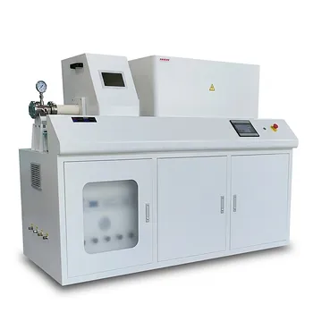
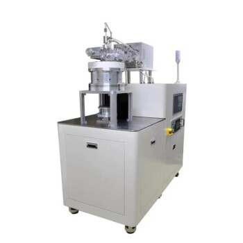
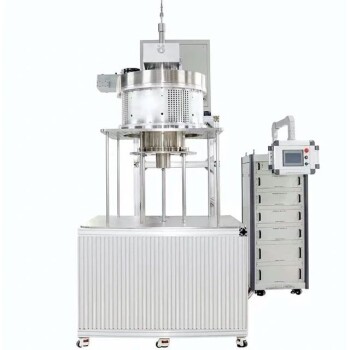
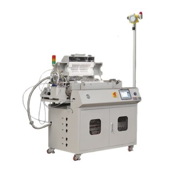
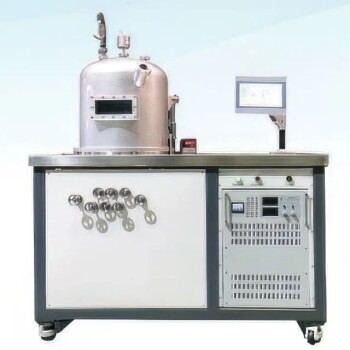
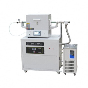
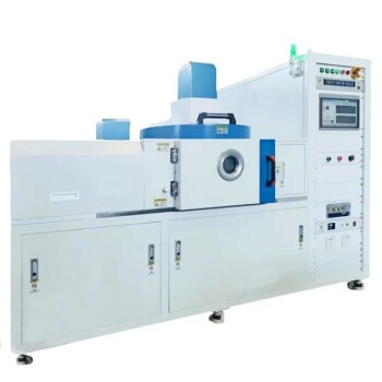
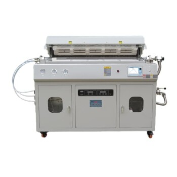
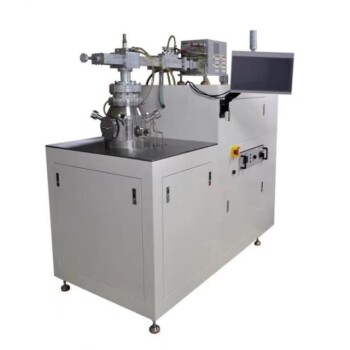
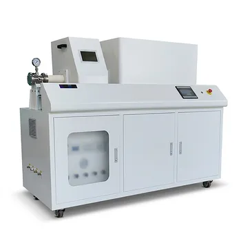
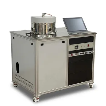
The primary role of a Chemical Vapor Deposition (CVD) system in Graphene FET fabrication is to synthesize large-area, high-quality monolayer graphene films. By reacting precursor gases on a metallic catalyst at high temperatures, the system creates the uniform, conductive channel material required for high-performance transistors. This process is currently the most successful method for producing graphene at the industrial scale necessary for modern semiconductor applications.
The CVD system acts as the foundational "bottom-up" manufacturing tool, transforming gaseous hydrocarbons into atomically thin films. Its precision in controlling temperature and gas ratios directly determines the electron mobility and structural integrity of the resulting Graphene FET.
The Synthesis Mechanism: From Gas to Graphene
Thermal Decomposition and Nucleation
The CVD process begins by introducing carbon-bearing precursor gases, such as methane, into a heated reaction chamber. At high temperatures, these gas molecules thermally decompose, releasing carbon atoms that settle onto a substrate.
The Role of the Metallic Catalyst
A metal substrate, typically copper (Cu) or nickel (Ni), serves as both a catalyst and a surface for the graphene lattice to form. The metal facilitates the chemical reaction and provides a template for the nucleation of the graphene lattice, ensuring the film grows into a continuous, high-quality structure.
Achieving Atomic Thickness
Advanced vacuum CVD systems manage the concentration of carbon sources to ensure the growth of a single layer of atoms. By maintaining specific pressures and cooling rates, the system prevents the formation of multi-layer "clumps," resulting in the monolayer graphene essential for FET performance.
Critical Parameters for FET Performance
Gas Ratio and Flow Control
The ratio of gases, particularly the balance between methane (the carbon source) and hydrogen, is vital for film quality. Hydrogen acts as an etchant that removes weak carbon bonds, helping to produce a film with low defect density and higher structural integrity.
Multi-Zone Temperature Management
Precise multi-zone temperature control ensures that the substrate is heated uniformly across its entire surface. Even minor fluctuations in temperature can lead to non-uniformity in the graphene film, which negatively impacts the electron mobility of the final transistor.
Surface Quality for Subsequent Experiments
The quality of the graphene grown via CVD is critical because it determines the performance of the device in subsequent tribological or electronic experiments. A high-quality surface ensures that the graphene can withstand the physical and electrical stresses of the fabrication process.
Understanding the Trade-offs and Challenges
The Complexity of the Transfer Process
While CVD grows graphene on metal, FETs usually require a different substrate, such as silicon. The transfer process—moving the graphene from the metal catalyst to the final device—is delicate and can introduce tears, wrinkles, or chemical residues.
Growth Speed vs. Defect Density
While CVD is relatively fast compared to other methods, accelerating the growth process can lead to increased grain boundaries. These boundaries act as obstacles to electron flow, potentially reducing the performance benefits of using graphene in the first place.
Substrate Compatibility and Cost
Using noble metals like Platinum (Pt) or Iridium (Ir) as catalysts can produce exceptionally high-quality graphene but significantly increases production costs. Copper remains the industry standard due to its balance of catalytic efficiency and cost-effectiveness.
How to Optimize CVD for Your Project Goals
Making the Right Choice for Your Goal
To achieve the best results with a CVD system in Graphene FET fabrication, consider your primary objective:
- If your primary focus is Maximum Electron Mobility: Prioritize a vacuum CVD system with precise multi-zone temperature control and high-purity copper catalysts to minimize lattice defects.
- If your primary focus is Industrial Scalability: Focus on optimizing the carbon source concentration and cooling rates to produce large-area films consistently across multiple batches.
- If your primary focus is Device Reliability: Invest in high-precision gas path management to ensure a stable methane-to-hydrogen ratio, which reduces structural inconsistencies in the monolayer.
By mastering the precise chemical and thermal environment of the CVD system, you can unlock the full potential of graphene for the next generation of high-speed electronics.
Summary Table:
| Key Feature | Role in Graphene FET Fabrication | Impact on Performance |
|---|---|---|
| Metallic Catalyst | Provides template for lattice nucleation (Cu/Ni) | High structural integrity |
| Precursor Gases | Delivers carbon source via thermal decomposition | Atomically thin uniformity |
| Gas Ratio Control | Hydrogen etching of weak carbon bonds | Low defect density |
| Multi-Zone Heating | Ensures uniform temperature across substrate | High electron mobility |
Elevate Your Semiconductor Research with KINTEK
Precision is the foundation of high-performance Graphene FETs. At KINTEK, we provide industry-leading CVD and PECVD systems designed for the atomic-scale accuracy your research demands. Our comprehensive range of laboratory solutions includes:
- Advanced CVD & PECVD Systems: For uniform, large-area graphene and carbon nanotube growth.
- High-Temperature Furnaces: Muffle, tube, vacuum, and atmosphere-controlled systems for precise thermal processing.
- Material Preparation: Crushing and milling systems, sieving equipment, and hydraulic presses (pellet, hot, isostatic).
- Specialized Lab Tools: High-pressure reactors, electrolytic cells, cooling solutions (ULT freezers, cold traps), and essential consumables like PTFE and ceramics.
Whether you are optimizing electron mobility or scaling production, KINTEK delivers the reliability and technical support you need. Contact our experts today to find the perfect CVD solution for your next-generation electronics!
References
- Gus Greenwood, Rosa M. Espinosa‐Marzal. Dynamically tuning friction at the graphene interface using the field effect. DOI: 10.1038/s41467-023-41375-7
This article is also based on technical information from Kintek Solution Knowledge Base .
Related Products
- Chemical Vapor Deposition CVD Equipment System Chamber Slide PECVD Tube Furnace with Liquid Gasifier PECVD Machine
- Microwave Plasma Chemical Vapor Deposition MPCVD Machine System Reactor for Lab and Diamond Growth
- 915MHz MPCVD Diamond Machine Microwave Plasma Chemical Vapor Deposition System Reactor
- Customer Made Versatile CVD Tube Furnace Chemical Vapor Deposition Chamber System Equipment
- HFCVD Machine System Equipment for Drawing Die Nano-Diamond Coating
People Also Ask
- What are the advantages of chemical vapor deposition? Achieve Superior Thin Films for Your Lab
- What types of substrates are used in CVD to facilitate graphene films? Optimize Graphene Growth with the Right Catalyst
- What is the chemical vapor deposition growth process? Build Superior Thin Films from the Atom Up
- How expensive is chemical vapor deposition? Understanding the True Cost of High-Performance Coating
- Why is Chemical Vapor Deposition (CVD) equipment uniquely suited for constructing hierarchical superhydrophobic structures?