At its core, the significance of Chemical Vapor Deposition (CVD) lies in its unique ability to "grow" materials atom by atom. It is a foundational process for creating exceptionally high-purity, uniform thin films on a substrate. This capability is indispensable for manufacturing advanced products like semiconductors, next-generation electronics, and durable cutting tools where material properties at the microscopic level dictate performance.
While many processes can simply coat a surface, CVD builds a new layer from the ground up using controlled chemical reactions. This fundamental difference gives engineers precise control over a material's structure, purity, and properties, enabling technologies that would otherwise be impossible.
The Core Principle: Building Materials from Gas
Chemical Vapor Deposition is less like painting a surface and more like coaxing frost to form in a very specific pattern and composition. It is a process of synthesis, not just application.
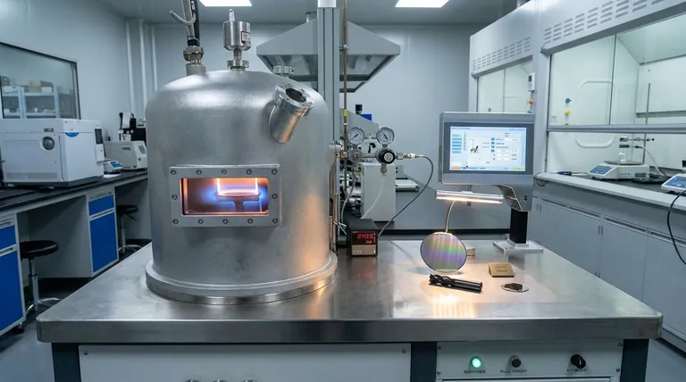
How CVD Works: From Gas to Solid
The process begins by introducing volatile precursor gases into a reaction chamber containing a heated substrate. When these gases come into contact with the hot surface, they undergo a chemical reaction or decomposition. The result is the deposition of a solid, high-purity thin film onto the substrate, with the remaining gaseous by-products being vented away.
Unparalleled Control Over Material Properties
The true power of CVD comes from its tunability. By precisely adjusting process parameters—such as temperature, pressure, gas mixture, and flow rates—engineers can dictate the final material's characteristics. This includes its chemical composition, thickness, crystal structure, and even grain size, allowing for the creation of highly engineered materials.
Key Applications Driven by CVD's Precision
CVD is not just a laboratory technique; it is the engine behind some of today's most advanced industries. Its significance is best understood through the products it enables.
Enabling Modern Electronics with Graphene
CVD is a leading method for producing large, high-quality sheets of graphene. For applications in high-performance electronics and transparent sensors, the ability to create films with low defects and excellent uniformity is critical. CVD delivers this by controllably depositing a single atomic layer of carbon.
Manufacturing Synthetic Diamond
Techniques like Microwave Plasma Chemical Vapor Deposition (MPCVD) have made it possible to synthesize high-quality diamond films. This has profound implications for both science and technology, providing a cost-effective source of one of the world's hardest and most thermally conductive materials for use in optics, electronics, and cutting tools.
Enhancing Industrial Durability with Hard Coatings
In heavy industry, CVD is used to apply ultra-hard coatings, such as titanium carbonitride (TiCN), onto carbide cutting tools. This process, known as Medium-Temperature CVD (MTCVD), dramatically increases a tool's lifespan and performance, especially in high-speed and heavy-duty cutting operations.
Understanding the Trade-offs and Limitations
No technology is without its challenges. The power of CVD comes with a specific set of operational complexities and constraints that must be managed.
The Challenge of High Temperatures
Traditional CVD processes often require very high temperatures (over 850°C). This can damage or deform many substrate materials, such as polymers or pre-fabricated electronic components, limiting the range of possible applications.
The Hazard of Precursor Chemicals
The precursor gases used in CVD are frequently toxic, flammable, or highly corrosive. This necessitates sophisticated handling protocols, robust safety systems, and significant investment in facility infrastructure to protect personnel and the environment.
The Problem of By-products
The chemical reactions that deposit the desired film also produce unwanted by-products. These substances are often hazardous themselves and require neutralization or specialized disposal methods, adding to the operational complexity and cost.
Mitigating the Drawbacks
To overcome the temperature limitation, variants like Plasma-Enhanced CVD (PECVD) or Laser-Assisted CVD have been developed. These methods use plasma or lasers to provide the energy needed for the reaction, allowing deposition to occur at much lower temperatures and broadening the range of compatible substrates.
Making the Right Choice for Your Goal
Deciding if CVD is the right process depends entirely on your project's end goal and constraints. Its precision is a powerful tool, but it is not always the necessary one.
- If your primary focus is ultimate material purity and structural perfection: CVD is often the superior choice for applications like advanced semiconductors or research-grade films where atomic-level control is non-negotiable.
- If your primary focus is coating complex 3D shapes uniformly: CVD's gas-phase nature gives it excellent "wrap-around" properties, allowing it to conformally coat intricate surfaces that are impossible for line-of-sight methods.
- If your primary focus is cost-sensitive coating on robust substrates: You must weigh the high performance of CVD against its operational costs and safety requirements, as simpler methods may be more economical if extreme purity is not the primary driver.
Ultimately, CVD is the technology you turn to when you need to construct a material with specific, engineered properties, not just apply a simple layer.
Summary Table:
| Key Aspect | Significance of CVD |
|---|---|
| Core Principle | Builds materials atom-by-layer via gas-phase chemical reactions. |
| Primary Advantage | Unparalleled control over film purity, thickness, and structure. |
| Key Applications | Semiconductors, graphene production, synthetic diamond, hard tool coatings. |
| Main Limitation | Often requires high temperatures and hazardous precursor gases. |
Need to engineer a high-purity thin film for your project?
KINTEK specializes in providing advanced lab equipment and consumables for precise processes like Chemical Vapor Deposition. Whether you are developing next-generation electronics or require durable coatings for industrial tools, our solutions help you achieve the material properties critical for success.
Contact our experts today to discuss how we can support your laboratory's specific needs.
Visual Guide

Related Products
- Chemical Vapor Deposition CVD Equipment System Chamber Slide PECVD Tube Furnace with Liquid Gasifier PECVD Machine
- RF PECVD System Radio Frequency Plasma-Enhanced Chemical Vapor Deposition RF PECVD
- Microwave Plasma Chemical Vapor Deposition MPCVD Machine System Reactor for Lab and Diamond Growth
- Customer Made Versatile CVD Tube Furnace Chemical Vapor Deposition Chamber System Equipment
- 915MHz MPCVD Diamond Machine Microwave Plasma Chemical Vapor Deposition System Reactor
People Also Ask
- What types of substrates are used in CVD to facilitate graphene films? Optimize Graphene Growth with the Right Catalyst
- What are the advantages of chemical vapor deposition? Achieve Superior Thin Films for Your Lab
- What are the processes of vapor phase deposition? Understand CVD vs. PVD for Superior Thin Films
- How expensive is chemical vapor deposition? Understanding the True Cost of High-Performance Coating
- Why is Chemical Vapor Deposition (CVD) equipment uniquely suited for constructing hierarchical superhydrophobic structures?


