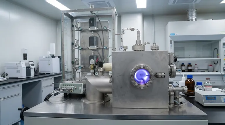
At its core, sputtering is a physical vapor deposition (PVD) technique, not a chemical one. It is a highly controlled process used to deposit an ultra-thin film of one material onto a surface, known as a substrate. This is achieved by placing a source material (the "target") and the substrate in a vacuum, introducing an inert gas like Argon, and creating a plasma that bombards the target, physically knocking its atoms loose to coat the substrate.
Sputtering should be understood not as a chemical reaction but as a microscopic game of billiards. It uses the physical momentum of energized gas ions to chip away atoms from a target material, allowing for the creation of exceptionally pure, dense, and strongly bonded thin films with precisely engineered properties.
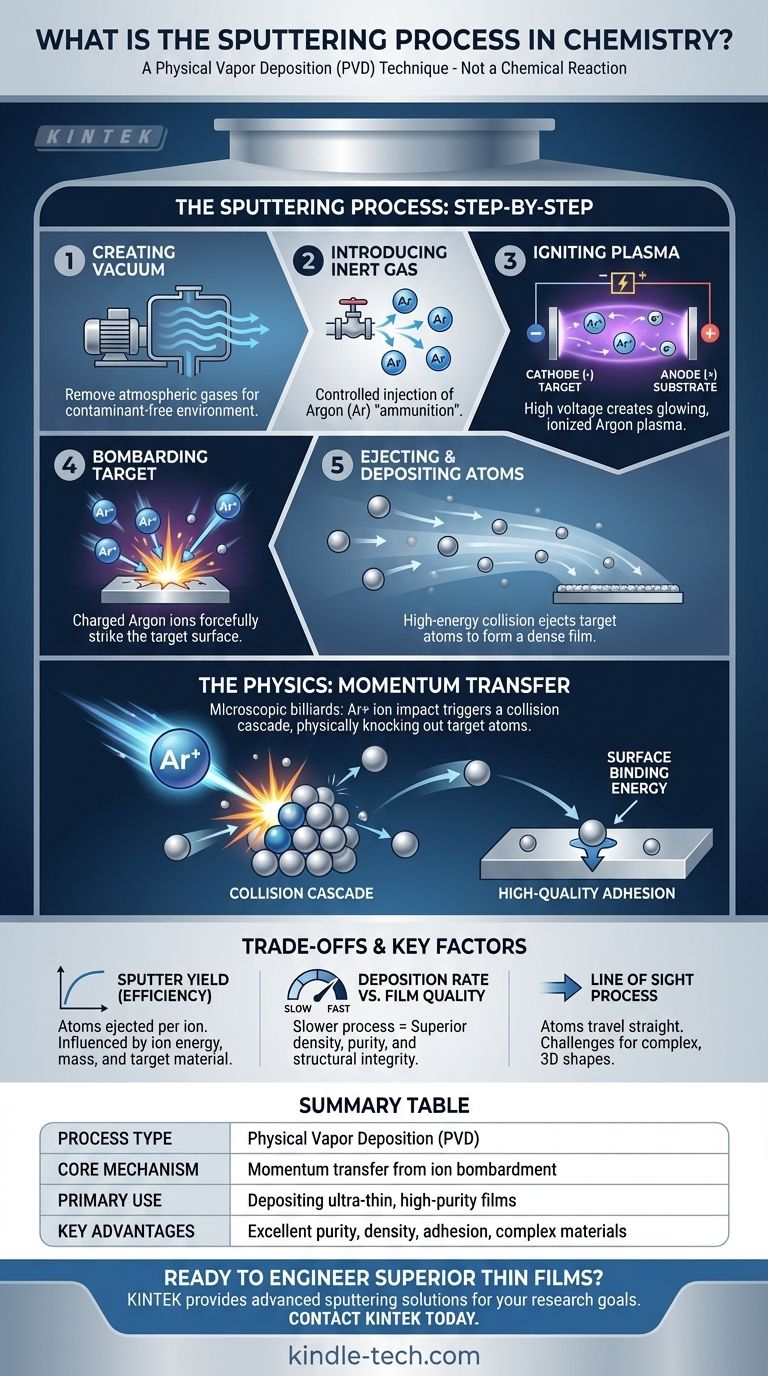
How Sputtering Works: A Step-by-Step Breakdown
The sputtering process relies on a sequence of physical events occurring within a controlled vacuum environment. Each step is critical to the final quality and characteristics of the deposited film.
Step 1: Creating the Vacuum Environment
The entire process takes place in a vacuum chamber. This is essential to remove atmospheric gases like oxygen and nitrogen, which would otherwise contaminate the film or react with the materials. The vacuum ensures the sputtered atoms can travel from the target to the substrate without unwanted collisions.
Step 2: Introducing an Inert Gas
A small, controlled amount of an inert gas, most commonly Argon (Ar), is introduced into the chamber. This gas is not meant to react with the materials; instead, it will be used as the "ammunition" for bombarding the target.
Step 3: Igniting the Plasma
A high voltage is applied between the target and the substrate, with the target acting as the cathode (negative). This strong electric field strips electrons from the Argon atoms, creating a glowing, ionized gas known as a plasma. This plasma is a mixture of positively charged Argon ions (Ar+) and free electrons.
Step 4: Bombarding the Target
The positively charged Argon ions are forcefully accelerated by the electric field and crash into the negatively charged target material. They strike the surface with significant kinetic energy.
Step 5: Ejecting and Depositing Atoms
This high-energy bombardment physically dislodges, or "sputters," individual atoms or molecules from the target material. This process creates a vapor stream of target atoms that travel across the chamber and land on the substrate, gradually building up a thin, uniform film.
The Physics of Sputtering: A Deeper Look
Understanding the underlying physics reveals why sputtering is such a powerful and precise technique for material engineering.
The Principle of Momentum Transfer
Unlike evaporation, which uses heat, sputtering relies purely on momentum transfer. When an energized Argon ion hits the target, it triggers a collision cascade within the material's atomic structure, similar to a cue ball breaking a rack of billiard balls.
Overcoming Surface Binding Energy
An atom is only ejected from the target if the chain reaction of collisions reaches the surface with enough energy to overcome the surface binding energy—the force holding the atoms together. This is a purely mechanical "knock-out" effect.
The Result: High-Quality Adhesion
The sputtered atoms arrive at the substrate with considerable kinetic energy, much higher than in thermal evaporation. This energy allows them to embed slightly into the substrate surface, forming a denser film with significantly stronger adhesion.
Understanding the Trade-offs and Key Factors
While powerful, sputtering is a complex process with specific advantages and limitations that determine its suitability for a given application.
Sputter Yield: The Measure of Efficiency
Sputter yield is the number of target atoms ejected per incident ion. This key metric is influenced by the ion's energy, its mass (heavier gases like Xenon can be more efficient), the angle of impact, and the binding energy of the target material itself.
Deposition Rate vs. Film Quality
Generally, sputtering is a slower deposition process compared to thermal evaporation. However, this slower, more energetic process typically results in films with superior density, purity, and structural integrity.
It's a "Line of Sight" Process
The sputtered atoms travel in a relatively straight line from the target to the substrate. This makes it challenging to uniformly coat complex, three-dimensional shapes without sophisticated machinery to rotate or move the substrate during deposition.
Making the Right Choice for Your Goal
Selecting sputtering depends entirely on the required properties of the final film. The process offers unparalleled control but comes with its own set of considerations.
- If your primary focus is high-purity, dense films: Sputtering is ideal because it preserves the exact composition of the source material without the fractional distillation effects seen in thermal evaporation of alloys.
- If your primary focus is coating with complex materials: Sputtering excels at depositing alloys, ceramics, and compounds that are difficult or impossible to melt and evaporate.
- If your primary focus is exceptional adhesion and durability: The high kinetic energy of sputtered atoms creates a stronger bond to the substrate, making it perfect for applications requiring robust coatings.
- If your primary focus is high-speed, low-cost deposition: You might explore simpler alternatives like thermal evaporation, especially for less demanding applications or simple metal coatings.
Understanding these principles empowers you to leverage sputtering not just as a coating technique, but as a precise tool for engineering materials at the atomic level.
Summary Table:
| Key Aspect | Description |
|---|---|
| Process Type | Physical Vapor Deposition (PVD) |
| Core Mechanism | Momentum transfer from ion bombardment (e.g., Argon) |
| Primary Use | Depositing ultra-thin, high-purity films on substrates |
| Key Advantages | Excellent film purity, density, adhesion, and ability to deposit complex materials like alloys and ceramics |
Ready to engineer superior thin films for your laboratory?
The sputtering process is a powerful tool for creating high-performance coatings with exceptional purity and adhesion. KINTEK specializes in providing advanced lab equipment and consumables, including sputtering systems, to meet the precise needs of research and development laboratories.
Our expertise ensures you get the right solution for depositing alloys, ceramics, and other complex materials with unmatched control. Let us help you achieve your material engineering goals with reliable, high-quality equipment.
Contact KINTEK today to discuss your specific application and discover how our sputtering solutions can enhance your research.
Visual Guide
Related Products
- Spark Plasma Sintering Furnace SPS Furnace
- High Temperature Muffle Oven Furnace for Laboratory Debinding and Pre Sintering
People Also Ask
- What is SPS sintering method? A Guide to High-Speed, High-Performance Material Fabrication
- What technical advantages does a Spark Plasma Sintering (SPS) furnace offer for LZP ceramics? Enhance Ionic Conductivity
- What are the fundamentals of spark plasma sintering process? Unlock Rapid, High-Performance Material Consolidation
- What is the pressure for spark plasma sintering? A Guide to Optimizing SPS Parameters
- What is the process fundamentals of spark plasma sintering? Achieve Rapid, High-Density Material Consolidation

