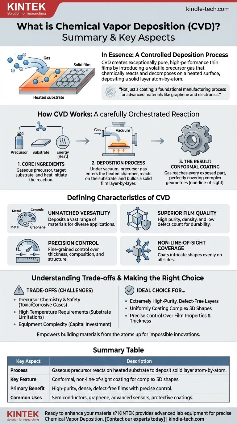
In essence, Chemical Vapor Deposition (CVD) is a highly controlled process for creating exceptionally pure, high-performance thin films and coatings. It works by introducing a volatile precursor gas into a chamber, which then chemically reacts and decomposes upon heating, depositing a solid layer atom-by-atom onto a target surface or substrate. This method allows for the creation of uniform, dense coatings on even the most complex shapes.
Chemical Vapor Deposition is not just a coating technique; it is a foundational manufacturing process valued for its precision and versatility, enabling the creation of advanced materials like graphene and the ultra-thin layers essential for modern electronics.
How Chemical Vapor Deposition Works
To understand the value of CVD, it’s essential to grasp its fundamental mechanism. The process is a carefully orchestrated chemical reaction on a surface, not just a simple spray-on application.
The Core Ingredients
The process begins with three key elements: a precursor, a substrate, and energy. The precursor is a chemical compound in a gaseous state that contains the elements you want to deposit. The substrate is the material or component you wish to coat. Energy, typically in the form of heat, is used to initiate the chemical reaction.
The Deposition Process
The substrate is placed inside a reaction chamber, which is typically under a vacuum. The precursor gas is then injected into the chamber. As the chamber is heated to a specific reaction temperature, the precursor gas breaks down or reacts on the hot substrate surface.
This chemical reaction leaves behind a solid material, which bonds directly to the substrate. Over time, this process builds up a thin, solid film one layer of atoms at a time.
The Result: A Conformal Coating
Because the precursor is a gas, it can reach every exposed part of the substrate. This results in a conformal coating, meaning it perfectly and uniformly covers all surfaces, including complex geometries, crevices, and internal bores. This "wrap-around" capability is a defining feature of CVD.
The Defining Characteristics of CVD
The unique nature of the CVD process gives it several powerful advantages that make it indispensable in high-technology manufacturing.
Unmatched Material Versatility
CVD is not limited to a single type of material. The process can be used to deposit a vast range of materials, including metal films, non-metal films, multi-component alloys, and complex ceramic compounds. It is a leading method for producing high-quality graphene for advanced sensors and electronics.
Superior Film Quality
The layer-by-layer deposition results in films that are exceptionally high in purity and density. Because the process is so controlled, the resulting coatings have a very low defect count, good crystallization, and low internal stress, making them highly durable and reliable.
Precision Control Over Properties
By carefully adjusting process parameters like temperature, pressure, and gas composition, operators have fine-grained control over the final product. This allows for precise tuning of the film's thickness (down to ultra-thin layers), chemical composition, crystal structure, and grain size.
Non-Line-of-Sight Coverage
Unlike processes that spray a material in a straight line, CVD is a non-line-of-sight technique. The gaseous precursor naturally fills the entire chamber, ensuring that even components with intricate and complex shapes are coated evenly on all sides.
Understanding the Trade-offs
While powerful, CVD is not a universal solution. An objective assessment requires acknowledging its operational demands and limitations.
Precursor Chemistry and Safety
The process relies on volatile precursor chemicals, which can be expensive, toxic, or corrosive. Handling and managing these gases require specialized equipment and stringent safety protocols.
High Temperature Requirements
Traditional CVD often requires very high temperatures to initiate the necessary chemical reactions. This can limit the types of substrates that can be coated, as the material must be able to withstand the heat without melting, warping, or degrading.
Equipment Complexity
While the concept is straightforward, the required equipment—including vacuum chambers, high-temperature furnaces, and precise gas delivery systems—can be complex and represent a significant capital investment.
Making the Right Choice for Your Goal
Selecting CVD depends entirely on your specific material and performance requirements.
- If your primary focus is creating extremely high-purity, defect-free layers: CVD is an ideal choice for applications like semiconductors and advanced sensors where material quality is non-negotiable.
- If your primary focus is uniformly coating complex, three-dimensional shapes: The conformal, non-line-of-sight nature of CVD makes it superior to many other coating methods for intricate components.
- If your primary focus is precise control over film thickness and composition: CVD offers unparalleled control, making it perfect for developing advanced materials or the ultra-thin layers required in electrical circuits.
Ultimately, Chemical Vapor Deposition empowers engineers and scientists to build materials from the atoms up, enabling innovations that would otherwise be impossible.
Summary Table:
| Key Aspect | Description |
|---|---|
| Process | Gaseous precursor reacts on a heated substrate to deposit a solid layer atom-by-atom. |
| Key Feature | Conformal, non-line-of-sight coating for complex 3D shapes. |
| Primary Benefit | High-purity, dense, and defect-free films with precise control. |
| Common Uses | Semiconductors, graphene production, advanced sensors, protective coatings. |
Ready to enhance your materials with high-purity coatings?
KINTEK specializes in providing the advanced lab equipment and consumables necessary for precise Chemical Vapor Deposition processes. Whether you are developing next-generation electronics or require durable, uniform coatings for complex components, our solutions are designed to meet the stringent demands of modern laboratories.
Contact our experts today to discuss how we can support your specific CVD application and help you achieve superior results.
Visual Guide
Related Products
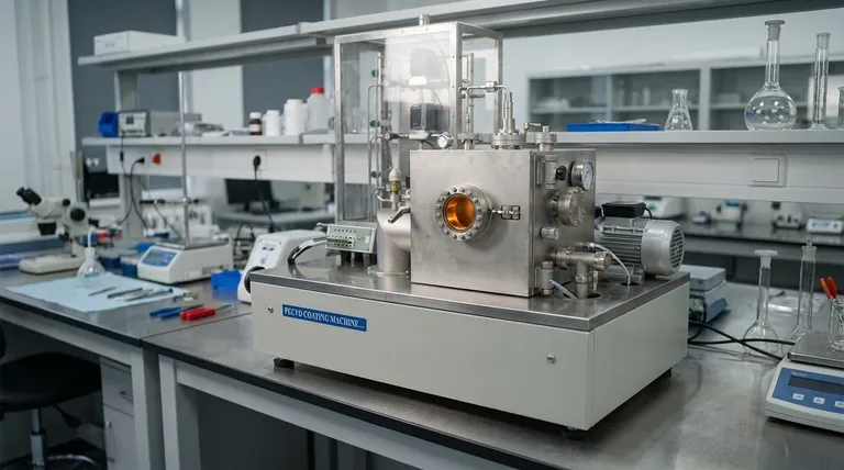
- Chemical Vapor Deposition CVD Equipment System Chamber Slide PECVD Tube Furnace with Liquid Gasifier PECVD Machine
- Customer Made Versatile CVD Tube Furnace Chemical Vapor Deposition Chamber System Equipment
- Microwave Plasma Chemical Vapor Deposition MPCVD Machine System Reactor for Lab and Diamond Growth
- 915MHz MPCVD Diamond Machine Microwave Plasma Chemical Vapor Deposition System Reactor
- Custom CVD Diamond Coating for Lab Applications
People Also Ask
- What happens during deposition chemistry? Building Thin Films from Gaseous Precursors
- What are the processes of vapor phase deposition? Understand CVD vs. PVD for Superior Thin Films
- What is the chemical vapor deposition growth process? Build Superior Thin Films from the Atom Up
- Why is Chemical Vapor Deposition (CVD) equipment uniquely suited for constructing hierarchical superhydrophobic structures?
- What are the advantages of chemical vapor deposition? Achieve Superior Thin Films for Your Lab


