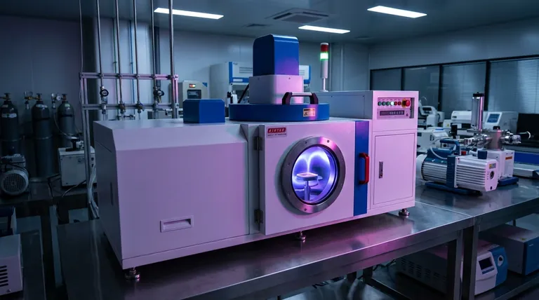
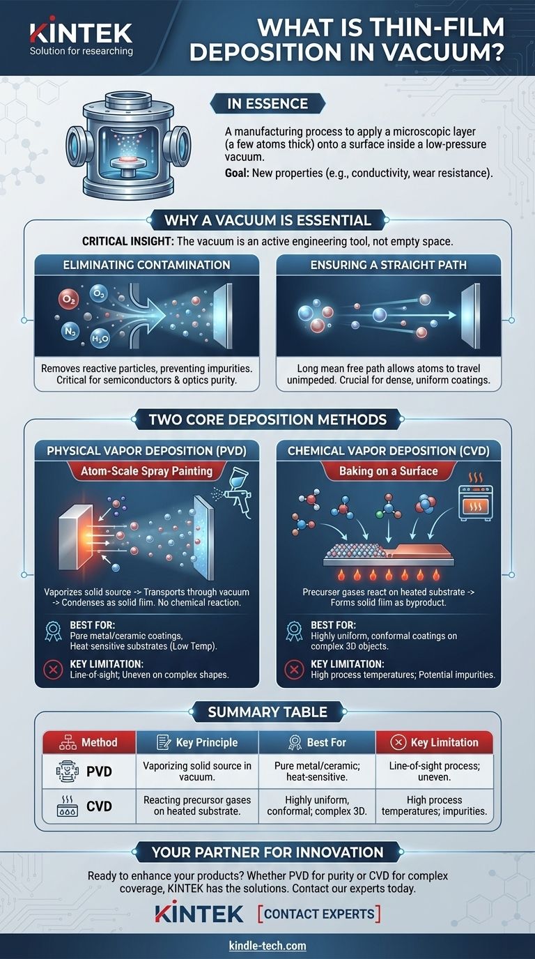
In essence, thin-film deposition in a vacuum is a manufacturing process used to apply a microscopic layer of material, often just a few atoms or molecules thick, onto a surface. This is done inside a low-pressure vacuum chamber to precisely control the film's properties, such as its purity, structure, and adhesion. The ultimate goal is to grant the surface new characteristics it did not originally have, like electrical conductivity, wear resistance, or specific optical properties.
The critical insight is that the vacuum is not merely an empty space; it is an active engineering tool. It eliminates atmospheric contaminants and allows atoms of the coating material to travel unimpeded, ensuring the deposited film is exceptionally pure and uniform.
Why a Vacuum is Essential for High-Quality Films
Creating a high-quality thin film is impossible in a normal atmosphere. The vacuum chamber environment is the key enabling factor that allows for the precision required at the atomic scale.
Eliminating Contamination
The air we breathe is filled with reactive particles like oxygen, nitrogen, and water vapor. These particles would immediately react with the depositing material, creating unwanted chemical compounds and introducing impurities into the film.
A vacuum removes these contaminants, ensuring the film is composed only of the intended material. This purity is critical for applications in semiconductors and optics.
Ensuring a Straight Path
In a vacuum, the mean free path—the average distance a particle can travel before colliding with another—is extremely long.
This means that atoms vaporized from the source material can travel in a straight, uninterrupted line to the target surface (the substrate). This line-of-sight travel is crucial for creating dense, uniform coatings.
The Two Core Deposition Methods
While there are many variations, nearly all vacuum deposition techniques fall into two fundamental categories: Physical Vapor Deposition (PVD) and Chemical Vapor Deposition (CVD).
Physical Vapor Deposition (PVD)
PVD is a process that turns a solid source material into a vapor, transports it through a vacuum, and condenses it onto the substrate as a solid film. This process does not involve a chemical reaction.
Think of it as atom-scale spray painting. A solid block of the coating material is either evaporated with heat or bombarded with ions to "blast" atoms off its surface. These atoms then coat whatever is in their path.
Chemical Vapor Deposition (CVD)
CVD involves introducing one or more precursor gases into the vacuum chamber. These gases decompose and react on the heated substrate's surface, forming the desired solid film as a byproduct.
This is more like baking a cake on a specific surface. The ingredients (gases) mix and undergo a chemical transformation only when they touch the hot surface (the substrate), creating a solid layer.
Understanding the Trade-offs
The choice between PVD and CVD is dictated by the desired film characteristics, the substrate material, and cost considerations. Neither method is universally superior.
PVD: Purity and Lower Temperatures
PVD often operates at lower temperatures than CVD, making it ideal for coating heat-sensitive materials like plastics. It excels at depositing very pure metals and simple ceramic coatings.
However, because PVD is largely a line-of-sight process, it can struggle to uniformly coat the inside of complex, three-dimensional shapes.
CVD: Conformal Coating and Higher Complexity
CVD's major advantage is its ability to produce highly conformal coatings. Because the precursor gases can flow around objects, CVD can evenly coat intricate and complex surfaces.
The downsides include the higher process temperatures, which can damage some substrates, and the potential for impurities to be left behind from the chemical reactions.
How to Apply This to Your Goal
Your specific application will determine the best path forward.
- If your primary focus is applying a pure metallic or hard ceramic coating to a relatively simple surface: PVD is often the more direct, pure, and lower-temperature solution.
- If your primary focus is uniformly coating a complex 3D object or a batch of small parts: CVD provides superior conformal coverage that a line-of-sight process like PVD cannot match.
- If your primary focus is protecting a heat-sensitive substrate like a polymer: The lower process temperatures of many PVD techniques make it the safer and more viable choice.
Understanding the fundamental difference between these physical and chemical pathways is the key to selecting the right technology for your specific engineering challenge.
Summary Table:
| Method | Key Principle | Best For | Key Limitation |
|---|---|---|---|
| Physical Vapor Deposition (PVD) | Vaporizing a solid source material in a vacuum. | Pure metal/ceramic coatings; heat-sensitive substrates. | Line-of-sight process; uneven coating on complex shapes. |
| Chemical Vapor Deposition (CVD) | Reacting precursor gases on a heated substrate. | Highly uniform, conformal coatings on complex 3D objects. | High process temperatures; potential for chemical impurities. |
Ready to enhance your products with precision thin-film coatings?
Whether you need the pure metallic coatings of PVD for sensitive materials or the uniform, complex coverage of CVD, KINTEK has the expertise and equipment to meet your specific laboratory and manufacturing challenges. Our solutions are designed to deliver the superior surface properties your projects demand.
Contact our experts today to discuss how our vacuum deposition solutions can drive your innovation forward.
Visual Guide
Related Products
- Molybdenum Tungsten Tantalum Evaporation Boat for High Temperature Applications
- Vacuum Hot Press Furnace Machine for Lamination and Heating
- Aluminized Ceramic Evaporation Boat for Thin Film Deposition
- Tungsten Evaporation Boat for Thin Film Deposition
- Electron Beam Evaporation Coating Oxygen-Free Copper Crucible and Evaporation Boat
People Also Ask
- What are thermal evaporation sources? Key Types and How to Choose the Right One
- Is thermal evaporation used to deposit a thin metal film? A Guide to This Foundational PVD Technique
- What is the source of evaporation for thin film? Choosing Between Thermal and E-Beam Methods
- What is thermal evaporation used to deposit? A Guide to Metals, Compounds, and Key Applications
- What are the sources of thermal evaporation? A Guide to Resistive vs. E-Beam Heating


