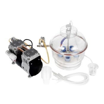
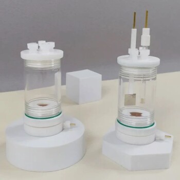
To be precise, the Chemical Vapor Deposition (CVD) method is not a technique that uses nanomaterials as inputs, but rather a powerful and versatile process used to synthesize or grow them from molecular precursors. It is extensively used to create a wide variety of high-purity, high-performance nanomaterials, with a particular strength in producing carbon-based structures like graphene, carbon nanotubes (CNTs), and carbon nanofibers (CNFs).
The core principle of CVD is its "bottom-up" approach. By precisely controlling gaseous chemicals (precursors) that react and deposit onto a heated surface (substrate), CVD allows for the atomic-level construction of highly ordered nanomaterials.
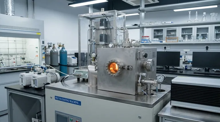
How the CVD Process Enables Nanomaterial Growth
Understanding the mechanism of CVD clarifies why it is so effective for creating specific types of nanomaterials. The process is a carefully orchestrated sequence of events.
The Role of Precursors
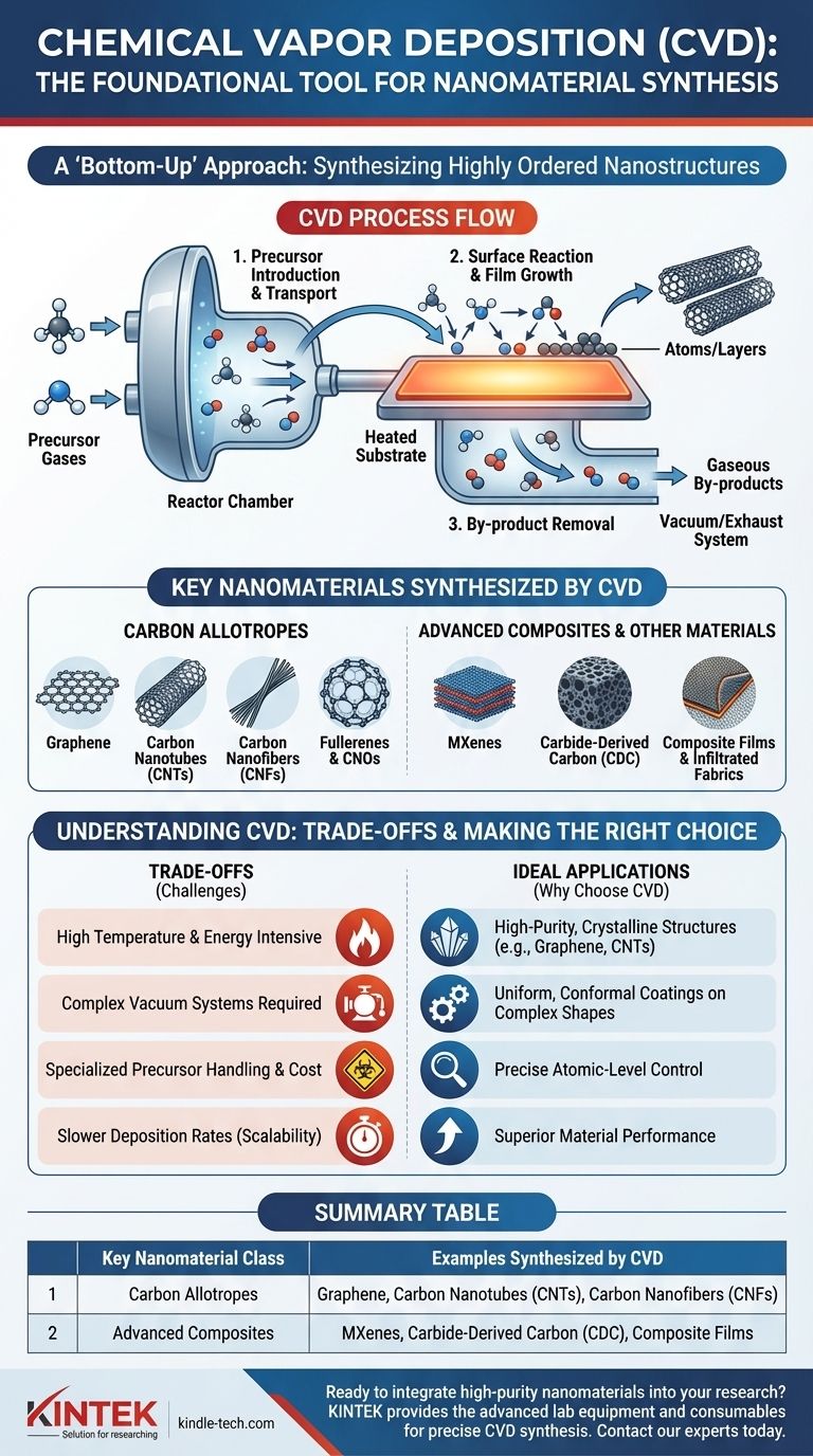
The synthesis begins by introducing precursor chemicals, typically in a gaseous state, into a reactor chamber. The choice of precursor is critical as it dictates the elemental composition of the final nanomaterial.
Transport to the Substrate
These gas molecules are transported towards a heated substrate. The high temperature of the substrate provides the energy needed to break chemical bonds and initiate reactions.
Surface Reaction and Film Growth
Precursor molecules adsorb (stick) to the hot substrate surface. They then decompose and react, depositing the desired solid material atom by atom or layer by layer, forming the nanostructure.
Removal of By-products
Gaseous by-products from the reaction are desorbed from the surface and removed from the reactor. This step is crucial for clearing the surface to allow for continuous, high-quality material growth.
Key Nanomaterials Synthesized by CVD
CVD is a dominant method for producing several classes of advanced nanomaterials, particularly those requiring a high degree of crystalline perfection.
Carbon Allotropes
This is the most well-known application of CVD. The method’s control over atomic deposition is ideal for building the specific bond structures of carbon.
- Graphene: Single sheets of carbon atoms arranged in a honeycomb lattice.
- Carbon Nanotubes (CNTs): Rolled-up sheets of graphene, forming hollow cylinders.
- Carbon Nanofibers (CNFs): Filaments with a structure similar to CNTs but often with a different arrangement of graphene planes.
- Fullerenes & Carbon Nano-onions (CNOs): Spherical carbon molecules and nested fullerene-like spheres.
Advanced Composite Materials
CVD is not limited to pure carbon. Its versatility allows for the creation of more complex materials and coatings.
- Carbide-Derived Carbon (CDC): A class of porous carbon materials synthesized from metal carbide precursors.
- MXenes: Two-dimensional inorganic compounds, typically carbides or nitrides of transition metals.
- Composite Films & Infiltrated Fabrics: CVD is also used to deposit thin films of a material onto a different substrate or to infiltrate porous structures like fabrics, creating advanced composite materials.
Understanding the Trade-offs of CVD
While powerful, CVD is not a universal solution. An objective evaluation requires acknowledging its inherent limitations.
High Temperature and Energy Requirements
Most CVD processes require very high temperatures to decompose the precursor gases and achieve high-quality crystal growth. This makes the process energy-intensive.
Need for Vacuum Systems
To ensure purity and prevent unwanted reactions with air, CVD is typically carried out under vacuum or in a controlled inert atmosphere, which requires complex and expensive equipment.
Precursor Handling and Cost
The gaseous precursors used in CVD can be expensive, highly toxic, or flammable, requiring specialized handling protocols and safety infrastructure.
Scalability and Deposition Rate
While excellent for producing high-quality materials, CVD can have slower deposition rates compared to other methods, which can be a challenge for large-scale, low-cost industrial production.
Making the Right Choice for Your Goal
Selecting a synthesis method depends entirely on your end goal. CVD excels in specific scenarios where its precision outweighs its complexity.
- If your primary focus is high-purity, crystalline structures like graphene or CNTs: CVD is the industry-standard method due to its unparalleled control over atomic-level growth.
- If your primary focus is creating uniform, conformal coatings on complex shapes: CVD's gas-phase deposition allows it to coat intricate surfaces evenly, making it superior to line-of-sight methods.
- If your primary focus is rapid, bulk production at the lowest possible cost: You should carefully evaluate the trade-offs, as methods like chemical exfoliation or arc discharge may offer higher throughput for certain nanomaterials, albeit often with lower quality.
Ultimately, Chemical Vapor Deposition is a foundational tool in nanotechnology, enabling the precise engineering of materials that drive innovation in electronics, energy, and medicine.
Summary Table:
| Key Nanomaterial Class | Examples Synthesized by CVD |
|---|---|
| Carbon Allotropes | Graphene, Carbon Nanotubes (CNTs), Carbon Nanofibers (CNFs) |
| Advanced Composites | MXenes, Carbide-Derived Carbon (CDC), Composite Films |
Ready to integrate high-purity nanomaterials into your research? KINTEK specializes in providing the advanced lab equipment and consumables needed for precise CVD synthesis. Our solutions empower laboratories to achieve superior material performance. Contact our experts today to discuss how we can support your specific nanotechnology goals.
Visual Guide
Related Products
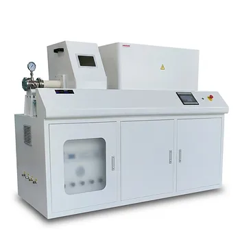
- Chemical Vapor Deposition CVD Equipment System Chamber Slide PECVD Tube Furnace with Liquid Gasifier PECVD Machine
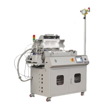
- Customer Made Versatile CVD Tube Furnace Chemical Vapor Deposition Chamber System Equipment
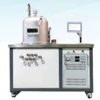
- HFCVD Machine System Equipment for Drawing Die Nano-Diamond Coating
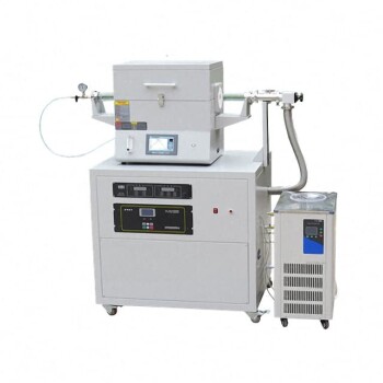
- Split Chamber CVD Tube Furnace with Vacuum Station Chemical Vapor Deposition System Equipment Machine
- Multi Heating Zones CVD Tube Furnace Machine Chemical Vapor Deposition Chamber System Equipment
People Also Ask
- What is plasma enhanced chemical vapor deposition PECVD equipment? A Guide to Low-Temperature Thin Film Deposition
- Why is Chemical Vapor Deposition (CVD) equipment uniquely suited for constructing hierarchical superhydrophobic structures?
- What are the advantages of chemical vapor deposition? Achieve Superior Thin Films for Your Lab
- What happens during deposition chemistry? Building Thin Films from Gaseous Precursors
- What are the core advantages of PE-CVD in OLED encapsulation? Protect Sensitive Layers with Low-Temp Film Deposition
