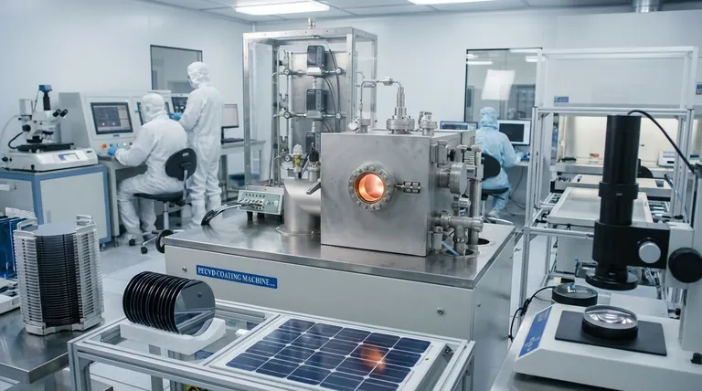
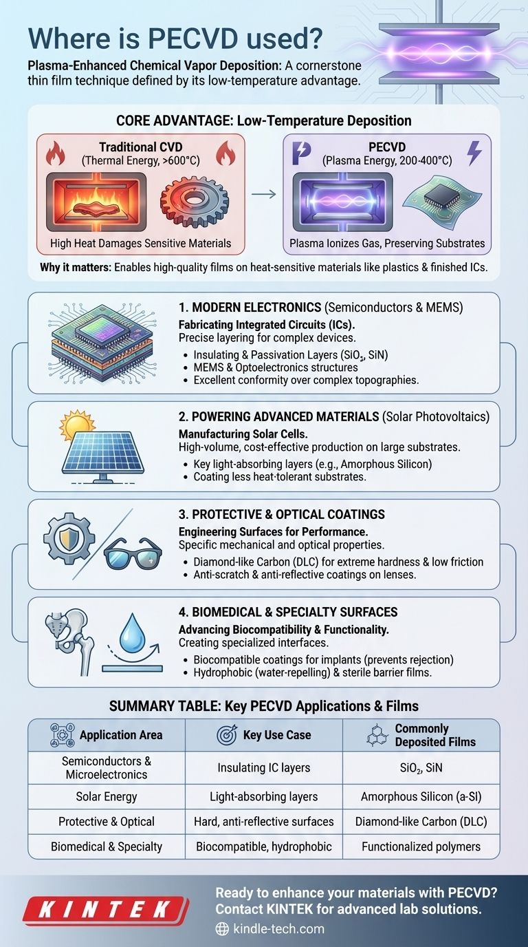
At its core, Plasma-Enhanced Chemical Vapor Deposition (PECVD) is a cornerstone fabrication technique used to deposit high-quality thin films across a vast range of industries. It is most prominently used in manufacturing semiconductors for integrated circuits and in the production of solar cells, but its applications extend to creating protective coatings for mechanical parts, optical layers for sunglasses, and biocompatible surfaces for medical implants.
The widespread use of PECVD is not just about the films it can create, but its unique ability to deposit them at low temperatures. This single advantage allows for the coating of heat-sensitive materials that would be destroyed by traditional high-temperature deposition methods, opening the door to countless modern technological applications.
The Foundation of Modern Electronics
PECVD is indispensable in the semiconductor industry, where the precise layering of materials on delicate silicon wafers is paramount. The process enables the creation of complex, multi-layered microelectronic devices.
Fabricating Integrated Circuits (ICs)
In microelectronics, devices are built layer by layer. PECVD is the go-to method for depositing dielectric films that insulate conductive components from one another.
Commonly deposited films include silicon dioxide (SiO₂) and silicon nitride (SiN). These layers serve as insulators, capacitors, and passivation layers that protect the device from environmental contaminants.
Building MEMS and Optoelectronics
Beyond standard ICs, PECVD is critical for fabricating Micro-Electro-Mechanical Systems (MEMS) and optoelectronic devices.
Its ability to create uniform, high-purity films with excellent conformity over complex topographies makes it ideal for these sophisticated, small-scale structures.
Powering and Protecting Advanced Materials
The low-temperature nature of PECVD extends its utility far beyond silicon wafers to a variety of substrates and functional needs.
Manufacturing Solar Cells (Photovoltaics)
PECVD plays a vital role in the solar industry. It is used to deposit key layers within photovoltaic cells, such as amorphous silicon.
The process enables the high-volume, cost-effective production of efficient solar panels by allowing deposition on large, often less heat-tolerant, substrates.
Developing Protective and Optical Coatings
PECVD is used to engineer surfaces with specific mechanical and optical properties. For example, Diamond-like Carbon (DLC) coatings are deposited on mechanical parts to provide extreme hardness and low friction.
In optics, it's used to create anti-scratch and anti-reflective coatings on lenses, sunglasses, and other optical components.
Advancing Biomedical and Specialty Surfaces
The versatility of PECVD allows for the creation of biocompatible coatings on medical implants, preventing rejection and improving device longevity.
It is also used to create specialized functional surfaces, such as hydrophobic (water-repelling) coatings for everything from pipelines to consumer electronics and sterile barrier films for food packaging.
Understanding the Core Advantage: Low-Temperature Deposition
The fundamental reason PECVD is so widely adopted is its unique process mechanics. It solves a critical limitation of conventional Chemical Vapor Deposition (CVD).
Why Temperature Is a Limiting Factor
Traditional CVD requires extremely high temperatures (often >600°C) to provide enough thermal energy to break down precursor gases and initiate film growth on a substrate.
These high temperatures would damage or destroy many materials, including plastics, polymers, and previously fabricated layers within a complex semiconductor device.
How Plasma Solves the Problem
PECVD generates an energy-rich plasma within the reaction chamber. This plasma, a state of ionized gas, provides the energy needed to decompose the precursor gases.
By using plasma energy instead of thermal energy, the deposition can occur at much lower temperatures (typically 200-400°C), well below the damage threshold for most sensitive materials.
The Benefit: High-Quality Films on Sensitive Substrates
This low-temperature capability allows manufacturers to gain the benefits of CVD—uniform, dense, and pure films—on a much wider array of substrates. This is what enables the coating of everything from plastic lenses to complex, multi-layered integrated circuits.
Matching the Application to the Need
Choosing a deposition method requires aligning the process capabilities with the final goal. PECVD's unique advantages make it the clear choice for specific scenarios.
- If your primary focus is microelectronics: PECVD is the industry standard for depositing high-quality insulating layers like silicon dioxide and silicon nitride on integrated circuits.
- If your primary focus is coating temperature-sensitive materials: PECVD is the definitive choice for applying high-performance films to substrates like polymers, plastics, or complex devices that cannot withstand high heat.
- If your primary focus is creating functional surfaces: PECVD provides a robust method for engineering surfaces with specific properties, such as the hardness of DLC or the water-repellency of hydrophobic coatings.
Ultimately, the low-temperature capability of PECVD is what unlocks its power, making it an essential tool for building the advanced materials that define modern technology.
Summary Table:
| Application Area | Key Use Case | Commonly Deposited Films |
|---|---|---|
| Semiconductors & Microelectronics | Insulating layers for integrated circuits (ICs) | Silicon Dioxide (SiO₂), Silicon Nitride (SiN) |
| Solar Energy (Photovoltaics) | Light-absorbing layers in solar cells | Amorphous Silicon (a-Si) |
| Protective & Optical Coatings | Hard, low-friction, or anti-reflective surfaces | Diamond-like Carbon (DLC) |
| Biomedical & Specialty Surfaces | Biocompatible or hydrophobic coatings | Functionalized polymer films |
Ready to enhance your materials with PECVD technology?
KINTEK specializes in advanced lab equipment and consumables for thin film deposition, serving the precise needs of research and industrial laboratories. Whether you are developing next-generation semiconductors, durable protective coatings, or innovative biomedical surfaces, our expertise and solutions can help you achieve superior film quality and process efficiency.
Contact us today to discuss how our PECVD solutions can accelerate your project and deliver the high-performance results you need.
Visual Guide
Related Products
- Inclined Rotary Plasma Enhanced Chemical Vapor Deposition PECVD Equipment Tube Furnace Machine
- Chemical Vapor Deposition CVD Equipment System Chamber Slide PECVD Tube Furnace with Liquid Gasifier PECVD Machine
- Inclined Rotary Plasma Enhanced Chemical Vapor Deposition PECVD Equipment Tube Furnace Machine
- RF PECVD System Radio Frequency Plasma-Enhanced Chemical Vapor Deposition RF PECVD
- Multi Heating Zones CVD Tube Furnace Machine Chemical Vapor Deposition Chamber System Equipment
People Also Ask
- What are the core advantages of PE-CVD in OLED encapsulation? Protect Sensitive Layers with Low-Temp Film Deposition
- How does plasma enhanced chemical vapor deposition work? Enable Low-Temperature Thin Film Deposition
- Why is a PECVD system required for vertical graphene synthesis? Master Directional Control for 3D Nanostructures
- What is plasma enhanced chemical vapor deposition PECVD equipment? A Guide to Low-Temperature Thin Film Deposition
- What are the benefits of plasma enhanced CVD? Achieve High-Quality, Low-Temperature Film Deposition


