Microwave plasma-generated radicals provide the necessary chemical energy to facilitate graphene growth where it naturally wouldn't occur. On non-catalytic substrates like glass or silicon, hydrogen-containing carbon radicals created by Microwave Surface Wave Plasma Chemical Vapor Deposition (MW-SWP CVD) diffuse to the surface, adsorb, and link together to form sp2-hybridized carbon structures. This process bypasses the need for metal catalysts by breaking precursor bonds in the plasma phase rather than on the substrate surface.
The high energy of microwave plasma compensates for the lack of surface catalytic activity on non-metallic materials. By generating reactive radicals in the gas phase, this method enables the direct assembly of graphene at relatively low temperatures without requiring a complex transfer process.
The Mechanism of Plasma-Enhanced Growth
Overcoming the Catalytic Gap
Non-metallic surfaces possess weak catalytic activity regarding the breakdown of carbon precursors. Unlike copper or nickel, substrates like glass cannot spontaneously fracture chemical bonds to initiate growth.
Microwave plasma acts as an external energy source to bridge this gap. It breaks the chemical bonds of the precursor gases before they ever touch the surface.
The Role of Carbon Radicals
The plasma environment generates hydrogen-containing carbon radicals. These are highly reactive species capable of forming chemical bonds immediately upon contact.
Because the precursors are pre-broken by the plasma's high energy, the substrate does not need to supply high thermal energy to activate the reaction.
Adsorption and Lattice Formation
Once generated, these radicals diffuse through the chamber and adsorb onto the substrate surface. They "stick" to the non-catalytic material, providing the building blocks for the material.
As they accumulate, they bond with one another to form sp2-hybridized carbon structures. This self-assembly results in the direct integration of a graphene layer onto the target material.
Understanding the Trade-offs
Process Complexity vs. Simplification
While this method simplifies the overall workflow by removing the transfer step, the physics of the plasma must be tightly controlled.
Energy Distribution
The high energy of the plasma allows for lower substrate temperatures, which is beneficial for delicate materials. However, if the plasma density is not uniform, it can lead to uneven growth or defects in the sp2 lattice structure.
Making the Right Choice for Your Goal
When deciding between direct plasma growth and traditional transfer methods, consider your specific constraints:
- If your primary focus is direct integration: Use plasma-enhanced growth to deposit graphene directly onto silicon or glass, avoiding the damage often caused by wet chemical transfers.
- If your primary focus is temperature sensitivity: Rely on the high energy of the radicals to drive the reaction, allowing you to keep the substrate at a lower temperature than thermal CVD requires.
By leveraging the reactivity of plasma-generated radicals, you can achieve functional graphene integration on virtually any dielectric surface.
Summary Table:
| Feature | Traditional Thermal CVD | MW-SWP CVD (Plasma-Enhanced) |
|---|---|---|
| Substrate Type | Catalytic metals (Cu, Ni) | Non-catalytic (Glass, Silicon, Dielectrics) |
| Bond Breaking | Occurs on substrate surface | Occurs in gas phase via plasma |
| Energy Source | High substrate temperature | High-energy microwave radicals |
| Transfer Step | Required (complex & risky) | Not required (direct growth) |
| Growth Temp | Typically high (>1000°C) | Lower temperatures possible |
Unlock Advanced Material Synthesis with KINTEK
Take your graphene research to the next level with precision-engineered equipment from KINTEK. Whether you are exploring CVD, PECVD, or MPCVD for direct graphene growth on non-catalytic substrates, or require high-performance crushing and milling systems for precursor preparation, we provide the tools necessary for scientific breakthroughs.
Our comprehensive portfolio supports your entire lab workflow:
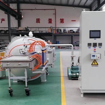
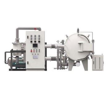
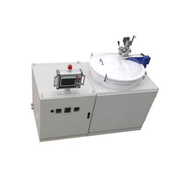
- High-Temperature Furnaces: Specialized vacuum and atmosphere systems for precise carbon deposition.
- Battery Research & Electrochemistry: Advanced electrolytic cells, electrodes, and testing tools.
- Material Processing: Hydraulic presses (pellet, isostatic) and high-pressure reactors/autoclaves for specialized synthesis.
- Lab Essentials: High-quality ceramics, crucibles, and PTFE products to ensure contamination-free results.
Ready to eliminate complex transfer processes and achieve superior material integration? Contact KINTEK today to consult with our experts on the perfect solution for your laboratory.
References
- Golap Kalita, Masayoshi Umeno. Synthesis of Graphene and Related Materials by Microwave-Excited Surface Wave Plasma CVD Methods. DOI: 10.3390/appliedchem2030012
This article is also based on technical information from Kintek Solution Knowledge Base .
Related Products
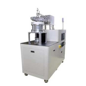
- Microwave Plasma Chemical Vapor Deposition MPCVD Machine System Reactor for Lab and Diamond Growth
- CVD Diamond Domes for Industrial and Scientific Applications
- CVD Diamond Dressing Tools for Precision Applications
- Laboratory CVD Boron Doped Diamond Materials
- Graphite Vacuum Continuous Graphitization Furnace
People Also Ask
- What is the microwave plasma enhanced chemical vapor deposition process? Achieve Low-Temperature, High-Quality Coatings
- What is the frequency of MPCVD? A Guide to Choosing 2.45 GHz vs. 915 MHz for Your Application
- How does Microwave Plasma Chemical Vapour Deposition (MPCVD) work? Your Guide to High-Purity Diamond Film Growth
- How plasma is used in diamond coating films? Unlock the Power of MPCVD for Superior Coatings
- What is the function of a Microwave PECVD system for Diamond Nanospikes? Precision 1-Step Nanostructure Synthesis
