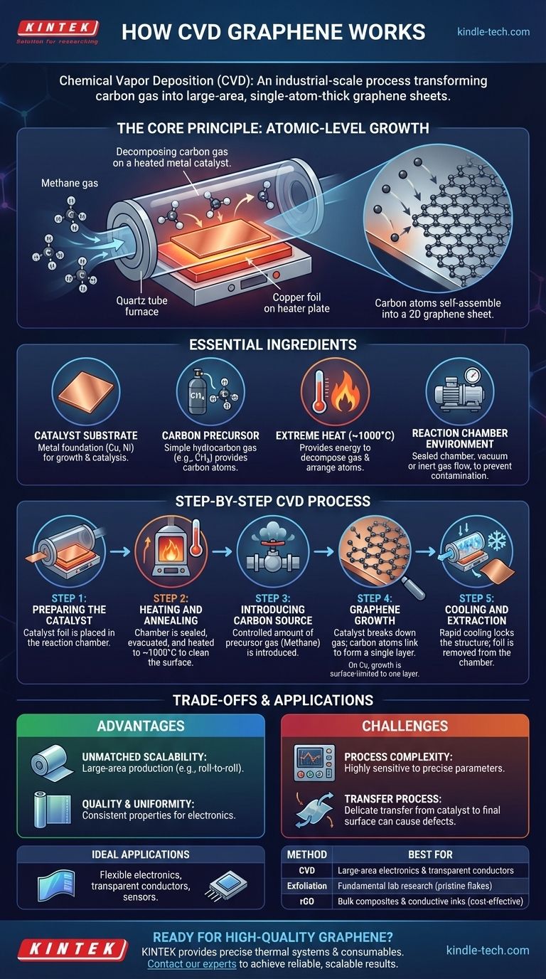
At its core, Chemical Vapor Deposition (CVD) for graphene is an industrial-scale fabrication process. It works by flowing a carbon-containing gas, such as methane, over a heated catalyst substrate, typically a copper or nickel foil. The high temperature breaks down the gas, allowing carbon atoms to deposit onto the metal surface and self-assemble into a continuous, single-atom-thick sheet of graphene.
The central concept behind CVD is transforming a simple, carbon-based gas into a highly structured, two-dimensional material. It is the only proven method capable of producing the large-area, high-quality graphene films necessary for advanced industrial applications like electronics and sensors.
The Core Principle: Building Graphene Atom by Atom
To understand how CVD works, you must first understand its three essential components. This process is less about assembly and more about controlled, atomic-level growth in a highly specific environment.
The Essential Ingredients
The recipe for CVD graphene relies on a precise combination of a substrate, a carbon source, and extreme heat.
- The Catalyst Substrate: A transition metal, most commonly copper (Cu) or nickel (Ni), serves as the foundation or "template" for graphene growth. Its surface provides the catalytic action needed to break down the carbon source.
- The Carbon Precursor: A simple hydrocarbon gas, like methane (CH₄), is used as the source for carbon atoms. When heated, this gas becomes reactive.
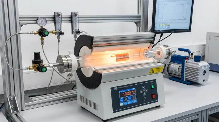
- The High Temperature: The entire process takes place in a furnace heated to around 1000 °C. This intense heat provides the energy required to decompose the precursor gas and allow carbon atoms to arrange themselves on the catalyst.
The Reaction Chamber Environment
This entire reaction must occur within a sealed chamber under a vacuum or a controlled flow of inert gases. This pristine environment is critical to prevent impurities from contaminating the growing graphene sheet, ensuring a pure and perfect final product.
A Step-by-Step Breakdown of the CVD Process
The CVD process is a delicate sequence of carefully controlled steps, each one critical to the final quality of the graphene film.
Step 1: Preparing the Catalyst
A thin foil of the catalyst metal, such as copper, is placed inside a quartz tube furnace, which serves as the reaction chamber.
Step 2: Heating and Annealing
The furnace is sealed, air is pumped out to create a vacuum, and it is heated to the target temperature of ~1000 °C. This high temperature prepares the metal's surface, removing oxides and creating a clean template for growth.
Step 3: Introducing the Carbon Source
Once the system is stable at the growth temperature, a small, controlled amount of the carbon precursor gas (methane) is introduced into the chamber.
Step 4: Graphene Growth on the Surface
The hot copper surface acts as a catalyst, breaking the methane molecules apart into carbon and hydrogen atoms. The carbon atoms then diffuse across the copper surface and link together into the iconic hexagonal lattice of graphene.
On copper, this growth is surface-limited, meaning it naturally stops once a complete single layer has formed, which is ideal for producing monolayer graphene.
Step 5: Cooling and Extraction
After a set period, the methane supply is cut off, and the system is rapidly cooled. This cooling process "locks" the graphene structure in place on the catalyst foil. The coated foil is then removed from the chamber.
Understanding the Trade-offs
While CVD is a powerful technique, it is essential to understand its advantages and the technical challenges it presents.
The Advantage: Unmatched Scalability
CVD is the only method capable of producing graphene on an industrial scale. Processes like roll-to-roll (R2R) production are being developed to create continuous sheets, making it suitable for commercial applications.
The Advantage: Quality and Uniformity
This method produces large, continuous films of graphene with uniform thickness, a critical requirement for applications in electronics, where consistent electrical properties across a surface are paramount.
The Challenge: Process Complexity
The quality of CVD graphene is highly sensitive to process parameters. Temperature, gas flow rates, pressure, and cooling speed must be monitored and controlled with extreme precision. Even minor deviations can introduce defects into the atomic lattice.
The Challenge: The Transfer Process
The graphene is grown on a metal foil, but it is almost always used on a different substrate (like silicon or plastic). The process of transferring this one-atom-thick film is incredibly delicate and a major source of tears, wrinkles, and impurities in the final product.
Making the Right Choice for Your Goal
Understanding the CVD process allows you to recognize where it fits within the broader landscape of graphene production methods.
- If your primary focus is large-area electronics or transparent conductors: CVD is the only viable method for producing the uniform, high-quality, and large-scale films your application requires.
- If your primary focus is fundamental research on small, pristine samples: Mechanical exfoliation (the "scotch tape" method) may be a simpler and faster way to obtain the highest-quality graphene flakes for lab-scale experiments.
- If your primary focus is creating bulk composites or conductive inks: Chemically derived materials like reduced graphene oxide (rGO) are often more cost-effective for applications where a large quantity of material is needed and perfect structure is less critical.
Ultimately, CVD is the critical technology that bridges the gap between graphene's discovery in the lab and its implementation in real-world devices.
Summary Table:
| Aspect | Key Detail |
|---|---|
| Core Process | Decomposing carbon gas (e.g., methane) on a heated metal catalyst (e.g., copper). |
| Key Advantage | Unmatched scalability for producing large-area, uniform, high-quality films. |
| Primary Challenge | Delicate transfer process from growth substrate to final application surface. |
| Ideal For | Industrial applications like flexible electronics, transparent conductors, and sensors. |
Ready to integrate high-quality graphene into your research or product development?
The controlled environment of a CVD process is key to success. KINTEK specializes in the lab equipment and consumables that power advanced materials science. Whether you need precise thermal systems for graphene growth or expert consultation on your setup, we are here to support your laboratory's innovation in 2D materials.
Contact our experts today to discuss how we can help you achieve reliable and scalable results.
Visual Guide
Related Products
- Carbon Graphite Plate Manufactured by Isostatic Pressing Method
- CVD Diamond for Thermal Management Applications
- Laboratory CVD Boron Doped Diamond Materials
- Custom CVD Diamond Coating for Lab Applications
- Vertical High Temperature Graphite Vacuum Graphitization Furnace
People Also Ask
- What is isostatic graphite? The Ultimate Material for High-Tech and High-Temperature Applications
- What is isostatic pressing in powder metallurgy? Unlock Superior Part Density and Complexity
- How big is the isostatic pressing market? A Deep Dive into the $1.2B+ Advanced Manufacturing Enabler
- What is the process of isostatic graphite manufacturing? Achieve Unmatched Material Uniformity and Performance
- What products are made by isostatic pressing? Achieve Flawless, High-Performance Components