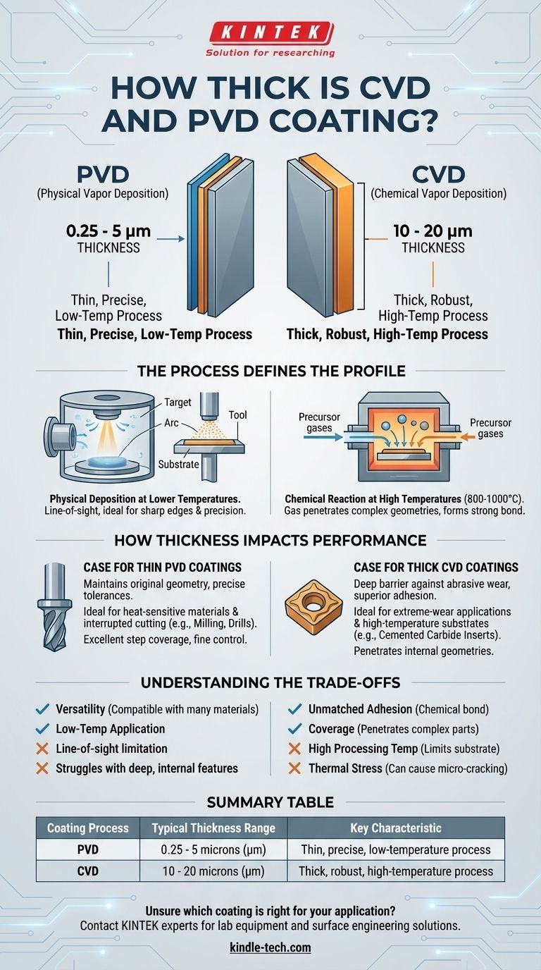
In practice, PVD coatings are typically thinner than CVD coatings. A Physical Vapor Deposition (PVD) coating generally ranges from 0.25 to 5 microns (μm). In contrast, a Chemical Vapor Deposition (CVD) coating is fundamentally a thicker film, often applied in a range of 10 to 20 microns. This significant difference in thickness is not arbitrary; it is a direct consequence of the two distinct manufacturing processes.
The choice between PVD and CVD is rarely about seeking a specific thickness. Instead, the decision hinges on the trade-offs between the high-temperature chemical reaction of CVD and the lower-temperature physical process of PVD, which in turn dictate the coating's final properties and suitability for your specific component.

The Process Defines the Profile
The thickness of a coating is intrinsically linked to how it is applied. PVD and CVD are fundamentally different methods, each with unique advantages and limitations that result in their characteristic thicknesses.
PVD: Physical Deposition at Lower Temperatures
Physical Vapor Deposition is a "line-of-sight" process conducted in a vacuum at relatively low temperatures. Solid source material is vaporized and then physically deposits onto the component's surface.
The resulting coating is thin, typically between 0.25 and 5 microns. This thinness allows for the preservation of sharp edges and precise dimensional tolerances, making it ideal for precision tools. The process parameters can be finely tuned to control characteristics like color, friction, and hardness.
CVD: Chemical Reaction at High Temperatures
Chemical Vapor Deposition uses precursor gases that react with the substrate surface at very high temperatures (800-1000°C). This process forms a new chemical bond between the coating and the part.
This chemical reaction allows for the formation of a much thicker and more tenaciously bonded layer, often in the 10 to 20 micron range. Unlike PVD, the gas can penetrate and coat all areas of a part, including complex non-line-of-sight geometries.
How Thickness Impacts Performance
The difference between a 2-micron PVD layer and a 15-micron CVD layer has profound implications for how a coated part will perform in its intended application.
The Case for Thin PVD Coatings
A thin PVD coating is ideal for applications where maintaining the part's original geometry is critical. Its lower application temperature makes it suitable for a wide range of substrates, including heat-sensitive tool steels that would be damaged by the CVD process.
This makes PVD the default choice for components like milling cutters, drills, and other tools used in interrupted cutting, where sharp edges and toughness are paramount.
The Case for Thick CVD Coatings
A thick CVD coating provides a deep, robust barrier against abrasive wear. Its exceptional hardness and superior adhesion make it the preferred choice for extreme-wear applications where the substrate material can tolerate the intense heat.
This is why CVD is commonly used on cemented carbide turning inserts for high-volume, continuous cutting of steel. The thick coating provides a longer tool life in highly abrasive environments.
Understanding the Trade-offs
Neither process is universally superior. The correct choice depends on balancing the inherent compromises of each technology.
CVD: Superior Adhesion vs. Thermal Stress
The primary strength of CVD is its unmatched adhesion, created by the chemical bond with the substrate.
However, its greatest weakness is the high processing temperature. This limits its use to materials that can withstand the heat, like cemented carbide. Furthermore, as the thick coating cools, significant tensile stress can build up, creating fine cracks. These cracks can propagate under impact, causing the coating to peel and making it unsuitable for high-impact or interrupted cutting operations.
PVD: Versatility vs. Coverage Limitations
PVD's main advantage is its versatility. The lower temperature makes it compatible with a vast array of materials, and the process offers fine control over the coating's final properties.
The key limitation is that it is a line-of-sight process. While it provides excellent, uniform coverage over external features and sharp edges ("step coverage"), it struggles to uniformly coat deep, complex internal geometries.
Making the Right Choice for Your Application
Selecting the right coating requires aligning the process with your material and performance goals.
- If your primary focus is precision on heat-sensitive materials: Choose PVD for its thin profile and low-temperature application.
- If your primary focus is maximum wear resistance on a heat-tolerant substrate: Choose CVD for its thick, chemically bonded layer.
- If your application involves interrupted cutting or high impact (e.g., milling): Choose PVD to avoid the internal stress and micro-cracking common in thick CVD coatings.
- If you need to coat complex internal geometries: Choose CVD, as its reactive gas can penetrate areas inaccessible to line-of-sight PVD.
Ultimately, the best coating is the one whose application process enhances your component's function without compromising the integrity of its base material.
Summary Table:
| Coating Process | Typical Thickness Range | Key Characteristic |
|---|---|---|
| PVD | 0.25 - 5 microns (μm) | Thin, precise, low-temperature process |
| CVD | 10 - 20 microns (μm) | Thick, robust, high-temperature process |
Unsure which coating is right for your application? The experts at KINTEK specialize in lab equipment and consumables for surface engineering. We can help you select the ideal coating process—whether it's thin, precise PVD for heat-sensitive tools or thick, durable CVD for extreme wear resistance. Contact our team today to discuss your specific requirements and enhance your component's performance.
Visual Guide
Related Products
- Custom CVD Diamond Coating for Lab Applications
- RF PECVD System Radio Frequency Plasma-Enhanced Chemical Vapor Deposition RF PECVD
- Electron Beam Evaporation Coating Oxygen-Free Copper Crucible and Evaporation Boat
- Vacuum Hot Press Furnace Machine for Lamination and Heating
- 1200℃ Split Tube Furnace with Quartz Tube Laboratory Tubular Furnace
People Also Ask
- What are diamond coated films? Enhance Materials with Super-Hard, Transparent Layers
- Is diamond coating worth it? Maximize Component Life and Performance
- What is CVD diamond coating? Grow a Super-Hard, High-Performance Diamond Layer
- How are tools coated with diamond? Achieve Superior Hardness and Low Friction for Your Tools
- What is the process of CVD diamond coating? Grow a Superior, Chemically-Bonded Diamond Layer