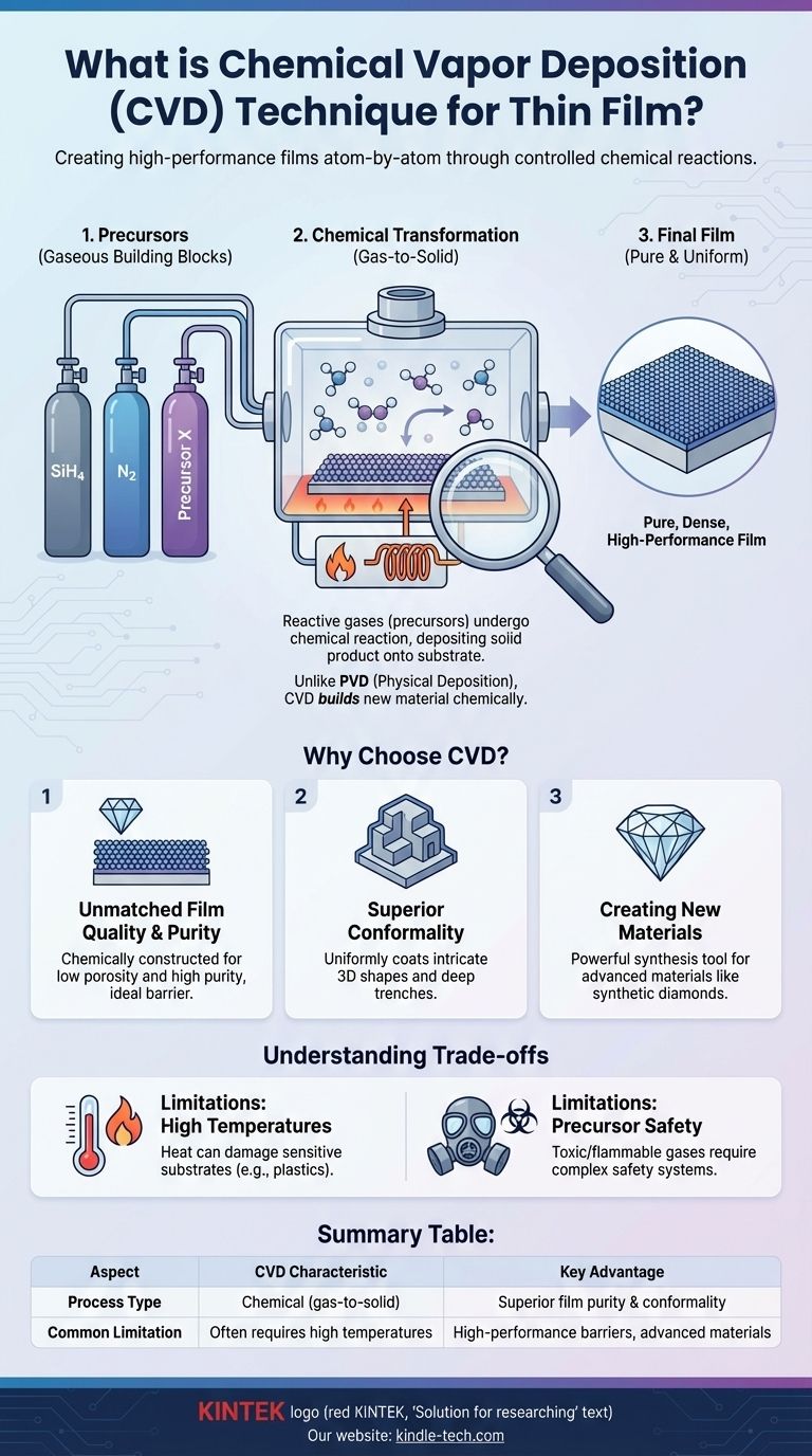
In essence, Chemical Vapor Deposition (CVD) is a process used to create high-performance thin films by making new materials directly on a surface. It works by introducing reactive gases (known as precursors) into a chamber, where they undergo a chemical reaction. The solid product of that reaction is then deposited as an exceptionally pure and uniform film onto a target object, known as a substrate.
While many methods simply coat a surface, CVD builds a new material atom-by-atom through controlled chemical reactions. This allows for the creation of exceptionally pure, dense, and high-performance films that are fundamentally integrated with the substrate, not just layered on top.
How CVD Fundamentally Works
To understand the power of CVD, it's crucial to grasp its core mechanism, which is more like baking than painting. You aren't applying a pre-made substance; you are creating a new one in place.
The Core Principle: A Chemical Transformation
At its heart, CVD is a gas-to-solid conversion process. Gaseous molecules are transported to a substrate where, prompted by energy (usually heat), they react and transform into a solid that bonds with the surface.
This process is distinct from Physical Vapor Deposition (PVD), the other major deposition technique, which typically involves physically blasting or evaporating a solid source material onto a substrate.
Precursors: The Gaseous Building Blocks
The process relies on precursors, which are carefully chosen gaseous raw materials. These gases contain the specific elements required to form the final film.
For example, to create a silicon nitride (Si₃N₄) film, gases like silane (SiH₄) and nitrogen (N₂) can be used as precursors.
The Reaction Environment
The entire process takes place inside a sealed reaction chamber. This controlled environment allows for precise management of temperature, pressure, and gas flow, which dictates the quality and properties of the final film.
Applying energy, most often high heat, provides the activation energy needed to break the chemical bonds in the precursor gases and drive the desired reaction on the substrate surface.
Why Choose CVD? The Key Advantages
Engineers and scientists choose CVD when the properties of the film are more critical than the cost or complexity of the process.
Unmatched Film Quality and Purity
Because the film is constructed chemically, it results in a material with extremely low porosity and a high degree of purity. This creates a dense, robust barrier that is ideal for protecting components from corrosion, water, or high temperatures.
Superior Conformality on Complex Shapes
A key advantage of CVD is its ability to uniformly coat complex, three-dimensional shapes. The precursor gases can flow into and access every small crevice and feature of a surface before they react.
The result is a film that is just as thick in a deep trench as it is on a flat surface—a property known as excellent conformality.
Creating Entirely New Materials
CVD is not just for protective coatings. It is a powerful synthesis tool used to create advanced materials. A prime example is the creation of synthetic diamonds, where carbon atoms from precursor gases are deposited layer by layer to grow a high-purity diamond.
Understanding the Trade-offs
No technique is perfect for every application. CVD's strengths come with specific limitations that are critical to understand.
High Temperatures Can Be a Limitation
Traditional CVD processes often require very high temperatures to initiate the chemical reactions. This heat can damage or destroy thermally sensitive substrates, such as plastics or certain electronic components.
Precursor Complexity and Safety
The gaseous precursors used in CVD can be highly toxic, flammable, or corrosive. This necessitates sophisticated and expensive safety and handling systems, increasing the overall complexity and cost of the operation compared to some PVD methods.
Making the Right Choice for Your Goal
Selecting a deposition method depends entirely on the desired outcome for your specific application.
- If your primary focus is ultimate film quality, purity, and density: CVD is the superior choice because its chemical process builds a near-perfect film from the ground up.
- If your primary focus is coating complex, three-dimensional shapes uniformly: CVD offers unmatched conformality, ensuring even coverage on the most intricate surfaces.
- If your primary focus is cost-effectiveness or the substrate is temperature-sensitive: You may need to explore alternatives like Physical Vapor Deposition (PVD) or specialized low-temperature CVD variants.
Ultimately, understanding CVD is about recognizing its power to chemically engineer materials directly onto a surface, opening up possibilities far beyond simple coating.
Summary Table:
| Aspect | CVD Characteristic |
|---|---|
| Process Type | Chemical (gas-to-solid) |
| Key Advantage | Superior film purity & conformality |
| Typical Application | High-performance barriers, advanced materials |
| Common Limitation | Often requires high temperatures |
Need a high-purity, conformal thin film for your project?
KINTEK specializes in advanced lab equipment, including CVD systems, to help you create superior coatings and materials. Our solutions are designed for precision, reliability, and performance, ensuring your research or production meets the highest standards.
Contact our experts today to discuss how CVD technology can benefit your specific application!
Visual Guide
Related Products
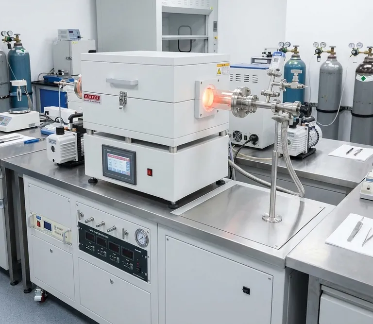
- Chemical Vapor Deposition CVD Equipment System Chamber Slide PECVD Tube Furnace with Liquid Gasifier PECVD Machine
- Customer Made Versatile CVD Tube Furnace Chemical Vapor Deposition Chamber System Equipment
- HFCVD Machine System Equipment for Drawing Die Nano-Diamond Coating
- 915MHz MPCVD Diamond Machine Microwave Plasma Chemical Vapor Deposition System Reactor
- Microwave Plasma Chemical Vapor Deposition MPCVD Machine System Reactor for Lab and Diamond Growth
People Also Ask
- Why is Chemical Vapor Deposition (CVD) equipment uniquely suited for constructing hierarchical superhydrophobic structures?
- What are the core advantages of PE-CVD in OLED encapsulation? Protect Sensitive Layers with Low-Temp Film Deposition
- What happens during deposition chemistry? Building Thin Films from Gaseous Precursors
- How expensive is chemical vapor deposition? Understanding the True Cost of High-Performance Coating
- What types of substrates are used in CVD to facilitate graphene films? Optimize Graphene Growth with the Right Catalyst


