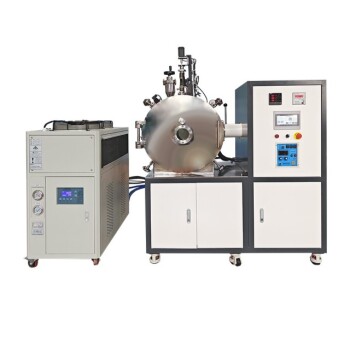
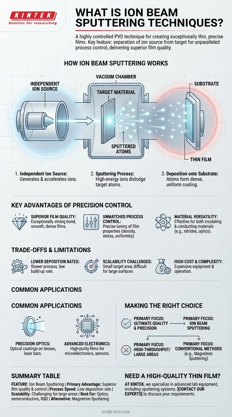
At its core, ion beam sputtering is a highly controlled physical vapor deposition (PVD) technique used to create exceptionally thin and precise films on a surface. It works by directing a focused beam of ions at a target material, which dislodges or "sputters" atoms from the target. These ejected atoms then travel through a vacuum and deposit onto a substrate, forming a dense, uniform, and high-quality coating.
The critical difference in ion beam sputtering is the separation of the ion source from the target material. This decoupling gives engineers unparalleled control over the deposition process, resulting in superior film quality at the expense of speed and scalability.
How Ion Beam Sputtering Works
The process is fundamentally about energy transfer, but its precision comes from how that energy is generated and directed. It is a refinement of general sputtering principles.
The Independent Ion Source
Unlike other methods where the plasma is generated near the target, ion beam sputtering uses an external, independent ion source. This source generates and accelerates ions, creating a well-defined, controllable beam.
The Sputtering Process
This focused beam of ions is directed at the target material inside a vacuum chamber. The high-energy impact of the ions transfers momentum to the target atoms, knocking them loose from the surface.
Deposition onto the Substrate
The sputtered atoms travel in a straight line until they strike the substrate—the component being coated. They condense on this surface, gradually building a thin film that can range from a few nanometers to several micrometers in thickness.
The Key Advantages of Precision Control
The separation of the ion source and target is not a minor detail; it is the source of the technique's primary advantages and why it's considered one of the best PVD methods available.
Superior Film Quality
The energy bonding of the deposited atoms is significantly higher than in standard vacuum coating, resulting in an exceptionally strong bond. The films produced are known for being extremely smooth and dense.
Unmatched Process Control
Because the ion source is independent, engineers can precisely control parameters like ion energy and beam current. This allows for fine-tuning the film's properties, such as its density, stress, and uniformity, with a high degree of precision.
Material Versatility
The process allows both insulating and conducting materials to be sputtered effectively. This flexibility makes it suitable for a wide range of advanced material applications, from nitride films to precision optics.
Understanding the Trade-offs and Limitations
No technique is without its drawbacks. The precision and quality of ion beam sputtering come at a significant cost in other areas.
Lower Deposition Rates
Ion beam sputtering is generally a much slower process compared to methods like magnetron sputtering. The rate at which the film builds up is low, making it less suitable for high-volume production.
Scalability Challenges
The focused nature of the ion beam results in a small target bombardment area. This makes it difficult and inefficient to deposit films of uniform thickness over large surface areas.
High Cost and Complexity
The equipment required for ion beam sputtering is complex and expensive to acquire and operate. This high barrier to entry reserves its use for applications where its unique benefits are absolutely necessary.
Common Applications Where Precision is Paramount
The trade-offs inherent in ion beam sputtering mean it is reserved for applications where film quality and control cannot be compromised.
Precision Optics
The technique is widely used for creating optical coatings on lenses, laser bars, and other components where uniformity and film density are critical for performance.
Advanced Electronics
In semiconductor production, ion beam sputtering is used to deposit the high-purity, defect-free thin films required for modern microelectronics and sensors, such as those found in gyroscopes.
Making the Right Choice for Your Goal
Selecting a deposition technique depends entirely on balancing the need for quality against the constraints of time and budget.
- If your primary focus is ultimate film quality and precision control: Ion beam sputtering is the superior choice for demanding applications in optics, semiconductors, or research.
- If your primary focus is high-throughput manufacturing or coating large areas: A more conventional method like magnetron sputtering will be far more practical and cost-effective.
Ultimately, ion beam sputtering is the expert's tool for when the atomic-level characteristics of a thin film are the most critical factor for success.
Summary Table:
| Feature | Ion Beam Sputtering |
|---|---|
| Primary Advantage | Superior film quality and precision control |
| Process Speed | Low deposition rate |
| Scalability | Challenging for large areas |
| Best For | Precision optics, semiconductors, R&D |
| Alternative for High-Volume | Magnetron Sputtering |
Need a high-quality thin film for a critical application?
At KINTEK, we specialize in providing advanced lab equipment, including sputtering systems, to meet the demanding needs of research and high-precision manufacturing. Our expertise can help you select the right PVD technology to achieve the exceptional film uniformity, density, and control required for your project in optics, semiconductors, or advanced materials.
Contact our experts today to discuss your specific requirements and discover how KINTEK's solutions can enhance your laboratory's capabilities.
Visual Guide
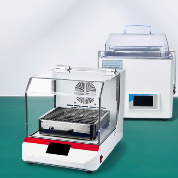
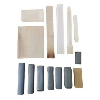
Related Products
- RF PECVD System Radio Frequency Plasma-Enhanced Chemical Vapor Deposition RF PECVD
- Electron Beam Evaporation Coating Oxygen-Free Copper Crucible and Evaporation Boat
- Chemical Vapor Deposition CVD Equipment System Chamber Slide PECVD Tube Furnace with Liquid Gasifier PECVD Machine
- Evaporation Boat for Organic Matter
- Hemispherical Bottom Tungsten Molybdenum Evaporation Boat
People Also Ask
- What is the principle of plasma enhanced chemical vapor deposition? Achieve Low-Temperature Thin Film Deposition
- What are the advantages of PECVD? Enable Low-Temperature, High-Quality Thin-Film Deposition
- What are the applications of PECVD? Essential for Semiconductors, MEMS, and Solar Cells
- How are PECVD and CVD different? A Guide to Choosing the Right Thin-Film Deposition Process
- What is plasma activated chemical vapour deposition method? A Low-Temperature Solution for Advanced Coatings