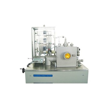
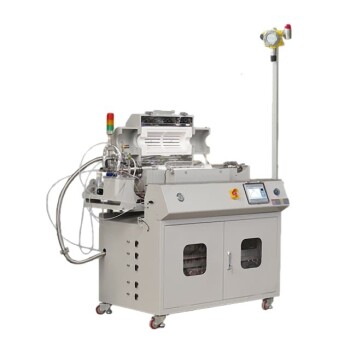
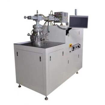
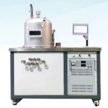
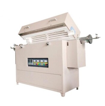
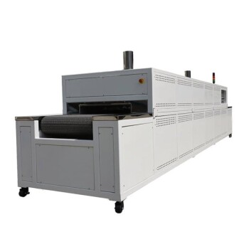
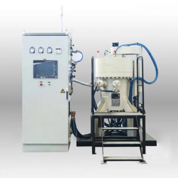
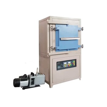
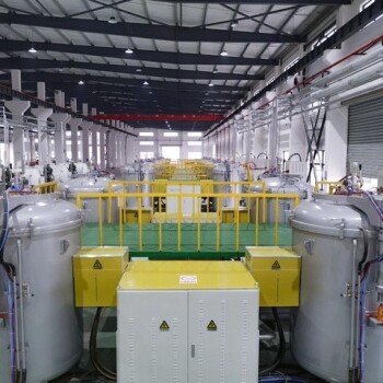
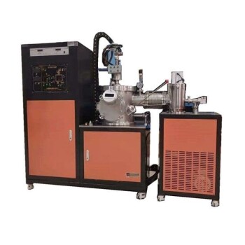
A Chemical Vapor Deposition (CVD) system functions as a high-precision manufacturing tool designed to grow high-purity tungsten thin films on specific substrates. By introducing volatile tungsten compounds—most notably tungsten hexafluoride—into a reaction chamber, the system induces high-temperature decomposition or reduction to deposit solid tungsten layers with exacting specifications.
The primary value of the CVD system lies in its ability to convert volatile gases into solid, structural layers, offering the distinct control over film thickness and crystal orientation necessary for high-performance engineering.
The Mechanism of Tungsten Deposition
The CVD process is not merely coating a surface; it is a chemical reaction engineered to occur at the substrate level. The system manages the environment to ensure uniform growth and purity.
Processing Volatile Compounds
The system begins by managing the flow of volatile tungsten compounds, such as tungsten hexafluoride.
These precursors are introduced into the chamber in a gaseous state, ensuring they can permeate complex geometries and cover the substrate evenly.
Decomposition and Reduction
Once inside the chamber, the system applies high temperatures.
This thermal energy triggers the decomposition or reduction of the gas. The chemical bonds of the precursor break down, leaving behind solid tungsten atoms that bond to the substrate, while byproducts are exhausted from the system.
Precision Control
A defining feature of the CVD system is its ability to regulate the deposition thickness.
Beyond thickness, the system also influences the crystal orientation of the tungsten film. This microstructural control is vital for defining the electrical and mechanical properties of the final material.
Critical Applications in Industry
The capability to deposit high-purity tungsten makes CVD systems indispensable in sectors requiring extreme durability or conductivity.
Microelectronic Interconnects
In semiconductor manufacturing, CVD systems are used to create interconnect layers.
Tungsten serves as a reliable conductor that connects different components within microelectronic devices. The precision of CVD ensures these connections are defect-free even at microscopic scales.
Nuclear Fusion Reactors
On a macro scale, these systems produce thermal shock-resistant coatings.
Specifically, CVD is used to coat the inner walls of nuclear fusion reactors. The deposited tungsten film must withstand immense heat and radiation without degrading, a feat achievable only through the high purity provided by CVD.
Understanding the Trade-offs
While CVD offers superior film quality, it involves specific operational challenges that must be managed.
Thermal Requirements
The process relies on high-temperature decomposition.
This requires significant energy input and limits the types of substrates that can be used, as the underlying material must withstand the processing temperatures without warping or melting.
Chemical Handling
The use of precursors like tungsten hexafluoride requires robust safety protocols.
The system must be equipped to safely handle volatile and potentially reactive gases, as well as effectively manage the exhaust of chemical byproducts resulting from the reduction process.
Making the Right Choice for Your Goal
When evaluating the role of a CVD system for tungsten fabrication, consider your specific end-use requirements.
- If your primary focus is Microelectronics: Prioritize the system's ability to control crystal orientation and thickness to ensure reliable electrical interconnects in dense circuitry.
- If your primary focus is High-Performance Coatings: Focus on the system's ability to produce high-purity, thermal shock-resistant films suitable for extreme environments like fusion reactor walls.
Ultimately, the CVD system is the standard for converting volatile tungsten chemistry into solid, high-performance engineering solutions.
Summary Table:
| Feature | Function in Tungsten CVD | Benefit |
|---|---|---|
| Precursor Management | Controls Tungsten Hexafluoride flow | Ensures uniform coverage of complex geometries |
| Thermal Control | High-temperature decomposition | Triggers precise chemical reaction at substrate |
| Structural Control | Regulates crystal orientation | Optimizes electrical and mechanical properties |
| Purity Management | Exhausts chemical byproducts | Delivers high-performance, defect-free layers |
Elevate Your Material Science with KINTEK CVD Systems
Are you looking to achieve superior tungsten film quality for semiconductors or extreme-environment engineering? KINTEK specializes in advanced CVD and PECVD systems designed for high-precision thin film deposition. Beyond our market-leading furnaces, we provide the complete laboratory ecosystem—from high-temperature reactors and crushing systems to isostatic presses and specialized ceramics—tailored to meet the rigorous demands of research and industrial production.
Ready to optimize your fabrication process? Contact KINTEK experts today for a consultation and custom solution!
References
- Samuel Omole, Alborz Shokrani. Advanced Processing and Machining of Tungsten and Its Alloys. DOI: 10.3390/jmmp6010015
This article is also based on technical information from Kintek Solution Knowledge Base .
Related Products
- RF PECVD System Radio Frequency Plasma-Enhanced Chemical Vapor Deposition RF PECVD
- Inclined Rotary Plasma Enhanced Chemical Vapor Deposition PECVD Equipment Tube Furnace Machine
- Customer Made Versatile CVD Tube Furnace Chemical Vapor Deposition Chamber System Equipment
- Multi Heating Zones CVD Tube Furnace Machine Chemical Vapor Deposition Chamber System Equipment
- Cylindrical Resonator MPCVD Machine System Reactor for Microwave Plasma Chemical Vapor Deposition and Lab Diamond Growth
People Also Ask
- What are the advantages of PECVD? Enable Low-Temperature, High-Quality Thin-Film Deposition
- What is plasma activated chemical vapour deposition method? A Low-Temperature Solution for Advanced Coatings
- What is the difference between PECVD and sputter? Choose the Right Thin-Film Deposition Method
- What are the benefits of PECVD? Achieve Superior Low-Temperature Thin Film Deposition
- How are PECVD and CVD different? A Guide to Choosing the Right Thin-Film Deposition Process

