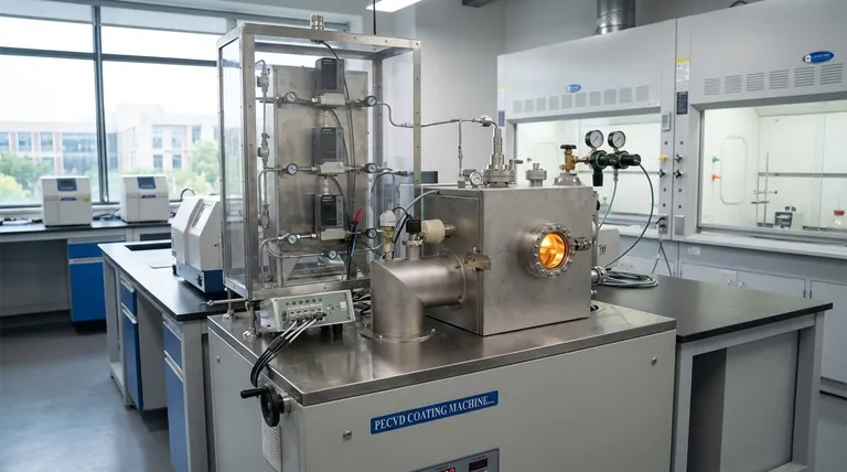
In essence, Chemical Vapor Deposition (CVD) is a sophisticated process used to create high-performance solid materials, typically as a thin film on a surface. It works by introducing specific gases, known as precursors, into a reaction chamber where they are energized and chemically react on a heated object (the substrate). This reaction deposits a new, solid layer of material directly onto the substrate's surface, building the film one atom or molecule at a time.
The core principle of CVD is not merely coating a surface, but rather constructing a new material from the ground up using gas-phase chemical reactions. The precise control of temperature, pressure, and gas chemistry allows for the creation of exceptionally pure and structured materials that are often impossible to produce by other means.
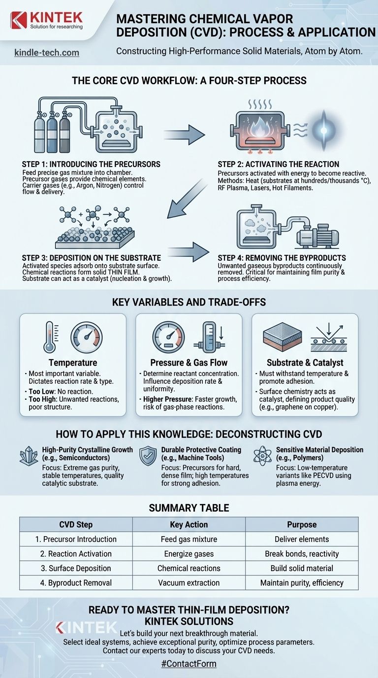
The Core CVD Workflow: A Four-Step Process
At its heart, every CVD process follows a fundamental sequence of events. Understanding these four steps provides a clear framework for how a gas mixture is transformed into a solid, functional film.
Step 1: Introducing the Precursors
The process begins by feeding a precise mixture of gases into a sealed reaction chamber containing the substrate. These precursor gases contain the chemical elements needed to form the final film.
Often, an inert carrier gas (like argon or nitrogen) is also used. This helps dilute the reactive gases and control their flow and uniform delivery to the substrate surface.
Step 2: Activating the Reaction
The precursor gases are stable at room temperature and must be activated with energy to become reactive. The most common method is heat, where the substrate is heated to hundreds or even thousands of degrees Celsius.
When the precursor gases contact the hot substrate, they gain the activation energy needed to break their chemical bonds. Other methods, such as RF plasma, lasers, or hot filaments, can also be used to energize the gases, sometimes allowing for lower substrate temperatures.
Step 3: Deposition on the Substrate
Once activated, the highly reactive gas molecules and atoms adsorb onto the substrate's surface. A series of chemical reactions takes place directly on this surface, causing the desired solid material to precipitate out and form a thin film.
The substrate is not always a passive surface. In many cases, such as the growth of graphene on a copper foil, the substrate acts as a catalyst, actively enabling and guiding the chemical reaction to form a specific crystalline structure. This process of forming and growing the film is called nucleation.
Step 4: Removing the Byproducts
The chemical reactions that form the solid film also create unwanted gaseous byproducts. These waste gases are continuously removed from the reaction chamber by a vacuum pump system.
Removing byproducts is critical for maintaining the purity of the film and ensuring the deposition reaction continues efficiently without being contaminated or inhibited.
Understanding Key Variables and Trade-offs
The quality, thickness, and properties of the final film are not accidental; they are the direct result of carefully managing several competing variables. Understanding these trade-offs is key to mastering the CVD process.
The Critical Role of Temperature
Substrate temperature is arguably the most important variable in CVD. It directly dictates the rate and even the type of chemical reaction that occurs.
Too low a temperature, and the reaction may not happen at all. Too high, and you may get unwanted reactions or a poorly structured, low-quality film.
Pressure and Gas Flow
The pressure inside the chamber and the flow rate of the precursor gases determine the concentration of reactants at the substrate surface. These factors directly influence the deposition rate (how fast the film grows) and its uniformity across the entire substrate.
Higher pressures can lead to faster growth but may also trigger unwanted gas-phase reactions before the precursors even reach the substrate.
Substrate and Catalyst Choice
The choice of substrate material is fundamental. It must be able to withstand the process temperature and have a surface that promotes the adhesion and desired growth of the film.
As mentioned, the substrate can also be a catalyst. In these cases, the surface chemistry of the substrate is just as important as the precursor gas chemistry in defining the final product.
How to Apply This Knowledge
Understanding the CVD process allows you to deconstruct its application for various goals. The "best" process is defined entirely by the desired outcome.
- If your primary focus is high-purity crystalline growth (e.g., semiconductors, graphene): Your success depends on extreme control over gas purity, stable temperatures, and the quality of the catalytic substrate.
- If your primary focus is a durable protective coating (e.g., on machine tools): The priority shifts to selecting precursor gases that create a hard, dense film and ensuring high temperatures that promote strong adhesion.
- If your primary focus is deposition on sensitive materials (e.g., polymers): The key is to use a low-temperature variant like Plasma-Enhanced CVD (PECVD), where energy from a plasma, not heat, drives the reaction.
Ultimately, CVD empowers engineers and scientists to design and build materials from the molecular level for a specific purpose.
Summary Table:
| CVD Step | Key Action | Purpose |
|---|---|---|
| Step 1: Precursor Introduction | Feed gas mixture into chamber | Deliver chemical elements for film formation |
| Step 2: Reaction Activation | Energize gases (heat/plasma) | Break chemical bonds to create reactivity |
| Step 3: Surface Deposition | Chemical reactions on substrate | Build solid material atom-by-atom |
| Step 4: Byproduct Removal | Vacuum pump extraction | Maintain film purity and process efficiency |
Ready to Master Thin-Film Deposition for Your Lab?
Understanding CVD is the first step. Implementing it successfully requires the right equipment and expertise. At KINTEK, we specialize in high-performance lab equipment and consumables for precise material synthesis.
We help you:
- Select the ideal CVD system for your specific application (semiconductors, protective coatings, or sensitive materials)
- Achieve exceptional film purity and controlled growth rates
- Optimize process parameters for your unique substrate requirements
Let's build your next breakthrough material together. Contact our experts today to discuss your CVD needs and discover how KINTEK solutions can accelerate your research and development.
Visual Guide
Related Products
- CVD Diamond Dressing Tools for Precision Applications
- Multi Heating Zones CVD Tube Furnace Machine Chemical Vapor Deposition Chamber System Equipment
- CVD Diamond Domes for Industrial and Scientific Applications
- CVD Diamond for Thermal Management Applications
- Chemical Vapor Deposition CVD Equipment System Chamber Slide PECVD Tube Furnace with Liquid Gasifier PECVD Machine
People Also Ask
- How long does it take to make synthetic diamonds? Discover the 6-8 Week Science Behind Lab-Grown Gems
- Does the chemical vapor deposition be used for diamonds? Yes, for Growing High-Purity Lab Diamonds
- What color diamonds are CVD? Understanding the Process from Brown Tint to Colorless Beauty
- What is CVD diamond? The Ultimate Guide to Lab-Grown Diamonds and Their Uses
- How do CVD diamonds grow? A Step-by-Step Guide to Lab-Grown Diamond Creation


