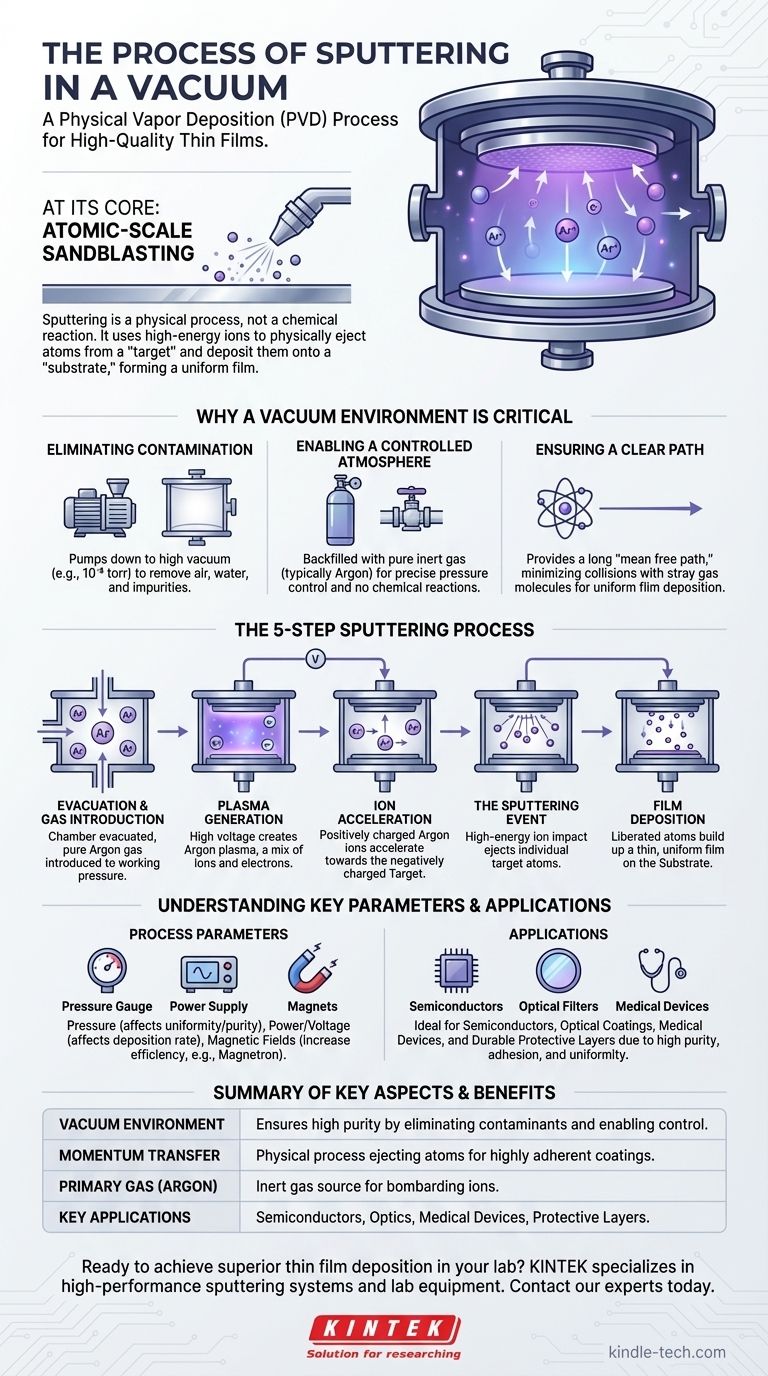
At its core, sputtering is a physical vapor deposition (PVD) process that functions like an atomic-scale sandblaster inside a high vacuum. In this process, a source material, known as the "target," is bombarded with high-energy ions from an inert gas. This collision has enough force to knock atoms loose from the target, which then travel through the vacuum and deposit onto a "substrate," forming an exceptionally thin, pure, and uniform film.
Sputtering is not a chemical reaction but a momentum transfer process. It uses the kinetic energy of ionized gas particles in a controlled vacuum to physically eject atoms from a source and deposit them as a highly adherent, ultra-thin coating onto another surface.
Why a Vacuum Environment is Critical
The entire sputtering process is performed under vacuum for two fundamental reasons: purity and control. Without it, the process would be unreliable and the resulting film would be compromised.
Eliminating Contamination
The initial step in any sputtering process is to pump down the chamber to a high vacuum (around 10⁻⁶ torr or lower). This removes air, water vapor, and other residual gas molecules that would otherwise react with the sputtered atoms or embed themselves as impurities in the final film.
Enabling a Controlled Atmosphere
Once a high vacuum is achieved, the chamber is backfilled with a small, precise amount of a high-purity inert gas, most commonly Argon. This gas is the source of the ions that will do the "blasting." A vacuum ensures that Argon is the only active gas present, preventing unwanted chemical reactions and giving operators precise control over the process pressure.
Ensuring a Clear Path
The low-pressure environment ensures that the sputtered atoms have a long "mean free path." This means they can travel from the target to the substrate with a minimal chance of colliding with stray gas molecules, which would scatter them and disrupt the uniformity of the film.
The Step-by-Step Sputtering Process
While the specifics can vary, the fundamental sequence involves creating ions, using them to bombard a target, and collecting the ejected atoms as a thin film.
Step 1: Evacuation and Gas Introduction
First, the deposition chamber containing the target material and the substrate is sealed and pumped down to a high vacuum to remove contaminants. Then, a carefully controlled amount of a sputtering gas, typically Argon, is introduced, raising the pressure slightly to a working level (e.g., 10⁻¹ to 10⁻³ mbar).
Step 2: Plasma Generation
A high voltage is applied within the chamber. This powerful electric field strips electrons from the Argon gas atoms, creating a mixture of positively charged Argon ions (Ar+) and free electrons. This ionized gas is known as a plasma, which often glows purple or blue.
Step 3: Ion Acceleration
The target material (the source of the coating) is given a strong negative electrical charge. This causes the positively charged Argon ions from the plasma to accelerate aggressively and collide with the negatively charged target surface.
Step 4: The Sputtering Event
When the high-energy Argon ions strike the target, they transfer their momentum to the target atoms. This impact is forceful enough to dislodge, or "sputter," individual atoms from the target material, ejecting them into the vacuum chamber.
Step 5: Film Deposition
The liberated atoms from the target travel through the low-pressure environment until they strike the substrate (the object being coated). Upon arrival, they condense and form a strong atomic-level bond, gradually building up a thin, uniform film layer by layer.
Understanding Key Process Parameters
The quality, thickness, and characteristics of the sputtered film are not accidental. They are the direct result of carefully controlling several variables during the process.
The Role of Pressure
The pressure of the sputtering gas inside the chamber is a critical trade-off. Higher pressure can increase the deposition rate but may decrease the uniformity and purity of the film due to increased atomic collisions.
The Impact of Power and Voltage
The voltage applied to the target directly influences the energy of the bombarding ions. Higher power levels increase the rate at which atoms are sputtered from the target, allowing for faster film deposition.
The Use of Magnetic Fields
Many modern sputtering systems are "magnetron" sputtering systems. Magnets are placed behind the target to create a magnetic field that traps the electrons from the plasma near the target's surface. This dramatically increases the efficiency of the ionization process, creating a denser plasma at lower pressures and leading to higher deposition rates.
Applying Sputtering to Your Goal
The choice to use sputtering is driven by the need for exceptionally high-quality thin films with specific properties.
- If your primary focus is an extremely durable and adherent coating: Sputtering creates a film with a virtually unbreakable bond to the substrate, ideal for wear-resistant and protective layers.
- If your primary focus is high purity and optical clarity: The vacuum environment is critical for preventing contamination, making sputtering a leading choice for optical filters, semiconductors, and medical devices.
- If your primary focus is creating a uniform film on a complex shape: Sputtering provides excellent, even coverage over intricate surfaces, far superior to many line-of-sight plating techniques.
Ultimately, sputtering provides an unparalleled level of control over the creation of thin films at the atomic level.
Summary Table:
| Key Aspect | Why It Matters |
|---|---|
| Vacuum Environment | Ensures high film purity by eliminating contaminants and enabling a controlled atmosphere. |
| Momentum Transfer | A physical (not chemical) process that ejects target atoms for a highly adherent coating. |
| Primary Gas | Argon is used as an inert gas to create ions that bombard the target material. |
| Key Applications | Ideal for semiconductors, optical coatings, medical devices, and durable protective layers. |
Ready to achieve superior thin film deposition in your lab?
KINTEK specializes in high-performance sputtering systems and lab equipment designed for precision and reliability. Whether you are developing semiconductors, optical coatings, or medical devices, our solutions deliver the high purity, uniformity, and adhesion your research demands.
Contact our experts today to discuss how we can support your specific laboratory needs and help you optimize your thin film processes.
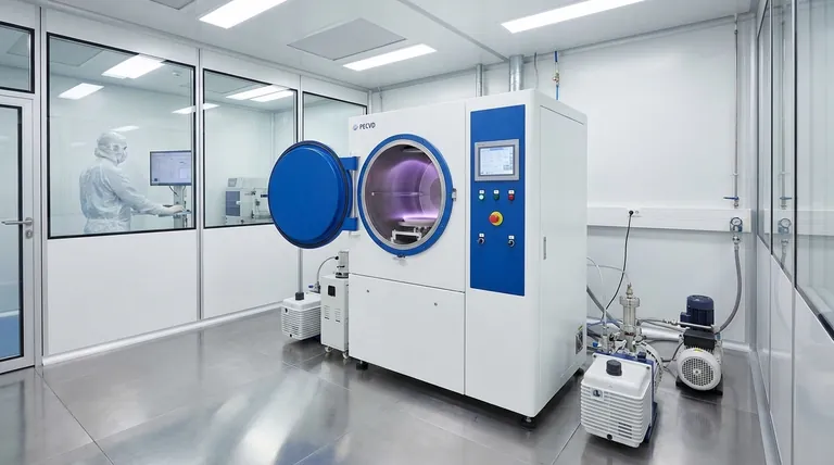
Visual Guide
Related Products
- HFCVD Machine System Equipment for Drawing Die Nano-Diamond Coating
- Vacuum Induction Melting Spinning System Arc Melting Furnace
- Vacuum Hot Press Furnace Machine for Lamination and Heating
- Split Chamber CVD Tube Furnace with Vacuum Station Chemical Vapor Deposition System Equipment Machine
- Chemical Vapor Deposition CVD Equipment System Chamber Slide PECVD Tube Furnace with Liquid Gasifier PECVD Machine
People Also Ask
- What are the disadvantages and challenges of the HFCVD method? Overcome Growth Limits and Filament Issues
- Why is Chemical Vapor Deposition (CVD) equipment uniquely suited for constructing hierarchical superhydrophobic structures?
- What is the chemical vapor deposition growth process? Build Superior Thin Films from the Atom Up
- What is the function of tungsten filaments in HFCVD? Powering Diamond Film Synthesis with Thermal Excitation
- What types of substrates are used in CVD to facilitate graphene films? Optimize Graphene Growth with the Right Catalyst