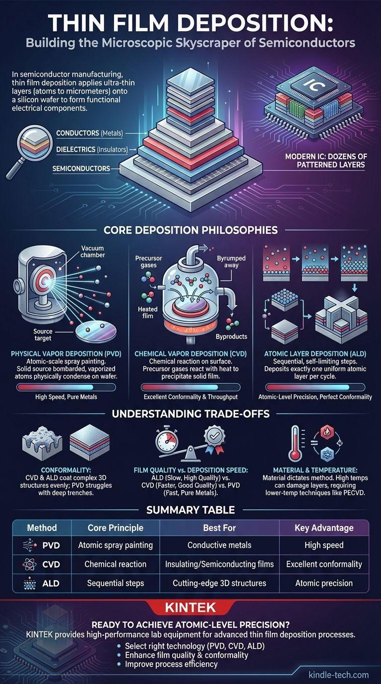
In semiconductor manufacturing, thin film deposition is the foundational process of applying an ultra-thin layer of material onto a silicon wafer. These layers, often only a few atoms to a few micrometers thick, are meticulously built up to form the functional electrical components—like transistors and wires—that constitute a modern integrated circuit.
The core purpose of thin film deposition is not merely to coat a surface, but to precisely construct the essential conductive, insulating, and semiconducting layers of a chip. The choice of deposition method is a critical engineering decision that directly dictates the final device's performance, power efficiency, and reliability.
The Goal: Building a Microscopic Skyscraper
Thin film deposition is the construction process for the microscopic, multi-level city that is an integrated circuit. Each layer has a specific purpose, and its quality is paramount.
From Bare Wafer to Complex Circuit
A finished chip is not a monolithic object but a stack of dozens of patterned layers. Thin film deposition is the process that creates each of these layers, one after another, on top of the underlying substrate or previous layer.
Modifying Electrical Properties
The primary goal in semiconductor fabrication is to control the flow of electricity. Deposition is used to create three fundamental types of layers:
- Conductors (Metals): Form the wires, or "interconnects," that shuttle signals between different components.
- Dielectrics (Insulators): Prevent electricity from leaking or short-circuiting between wires and components.
- Semiconductors: Form the transistors, the on/off switches that are the basis of digital logic.
The Critical Need for Purity and Precision
On the nanoscale, there is no margin for error. The performance of a modern transistor can be severely degraded by a few misplaced atoms or a slight impurity in a deposited film. As chip features shrink, the demand for atomic-level perfection in these films becomes ever more intense.
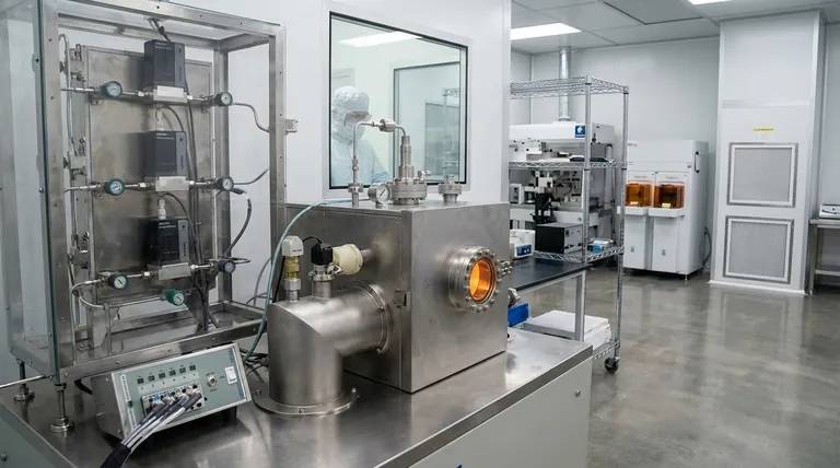
Core Deposition Philosophies
While many techniques exist, they generally fall into two major families: Physical Vapor Deposition (PVD) and Chemical Vapor Deposition (CVD).
Physical Vapor Deposition (PVD)
Think of PVD as a form of atomic-scale spray painting. A solid source material (a "target") is bombarded with energy inside a vacuum, causing atoms to be ejected. These vaporized atoms travel in a straight line and physically condense onto the cooler wafer, forming a thin film.
Chemical Vapor Deposition (CVD)
CVD is more like baking. Precursor gases containing the required atoms are introduced into a chamber with the wafer. A chemical reaction, often induced by heat, occurs on the wafer's surface, causing the desired atoms to "precipitate" out of the gas and form a solid film. Unwanted byproducts are pumped away.
Atomic Layer Deposition (ALD)
ALD is a highly advanced, sequential form of CVD. It breaks the process into self-limiting steps, depositing exactly one uniform layer of atoms per cycle. This provides unparalleled control over film thickness and uniformity, which is essential for creating the most complex, three-dimensional transistor structures in leading-edge chips.
Understanding the Trade-offs
No single deposition method is perfect for every application. Engineers must choose based on a clear set of trade-offs.
Conformality: Covering Complex Topography
Conformality describes how well a film covers a textured surface. CVD and ALD are highly conformal, meaning they can deposit a uniform layer over complex 3D structures. PVD is a line-of-sight process and struggles to evenly coat the sidewalls and bottoms of deep trenches.
Film Quality vs. Deposition Speed
Generally, slower processes yield higher-quality films. ALD provides the highest possible quality and control but is also the slowest. Certain types of CVD offer a balance of good quality at a much faster rate, making them suitable for thicker films where atomic precision is less critical.
Material and Temperature Constraints
The material being deposited dictates the available methods. Furthermore, the deposition temperature is a major concern. High temperatures can damage previously fabricated layers on the chip, forcing engineers to use lower-temperature techniques like Plasma-Enhanced CVD (PECVD) for later steps in the manufacturing flow.
Matching the Method to the Application
Your choice of deposition technology is dictated entirely by the layer's function within the chip's architecture.
- If your primary focus is creating conductive metal interconnects: PVD is often the workhorse for efficiently depositing pure metal layers, especially for the main wiring levels.
- If your primary focus is depositing uniform insulating or semiconducting films: A form of CVD is typically the best choice, offering a great balance of film quality, conformality, and throughput.
- If your primary focus is building cutting-edge 3D transistor gates and high-k dielectrics: ALD is non-negotiable for its atomic-level precision and perfect ability to coat complex, nanoscale features.
Ultimately, mastering thin film deposition is mastering the art of building functional matter, one atomic layer at a time.
Summary Table:
| Method | Core Principle | Best For | Key Advantage |
|---|---|---|---|
| PVD (Physical Vapor Deposition) | Atomic-scale spray painting in a vacuum | Conductive metal interconnects | High deposition speed for pure metals |
| CVD (Chemical Vapor Deposition) | Chemical reaction on wafer surface | Uniform insulating/semiconducting films | Excellent conformality and throughput |
| ALD (Atomic Layer Deposition) | Sequential, self-limiting reactions | Cutting-edge 3D transistor gates | Atomic-level precision and uniformity |
Ready to achieve atomic-level precision in your semiconductor fabrication?
At KINTEK, we specialize in providing high-performance lab equipment and consumables tailored for advanced thin film deposition processes. Whether you're developing next-generation chips or optimizing your current production line, our solutions ensure the purity, precision, and reliability your research demands.
We help you:
- Select the right deposition technology (PVD, CVD, ALD) for your specific application.
- Enhance film quality and conformality to meet the challenges of shrinking chip features.
- Improve process efficiency with reliable equipment and expert support.
Let's build the future of electronics, one atomic layer at a time. Contact our experts today to discuss your semiconductor manufacturing needs!
Visual Guide
Related Products
- Inclined Rotary Plasma Enhanced Chemical Vapor Deposition PECVD Equipment Tube Furnace Machine
- HFCVD Machine System Equipment for Drawing Die Nano-Diamond Coating
- 915MHz MPCVD Diamond Machine Microwave Plasma Chemical Vapor Deposition System Reactor
- CVD Diamond Cutting Tool Blanks for Precision Machining
- Vacuum Hot Press Furnace Machine for Lamination and Heating
People Also Ask
- What is the difference between CVD and PECVD? Choose the Right Thin-Film Deposition Method
- What is plasma in CVD process? Lowering Deposition Temperatures for Heat-Sensitive Materials
- What materials are deposited in PECVD? Discover the Versatile Thin-Film Materials for Your Application
- How does plasma enhanced CVD work? Achieve Low-Temperature, High-Quality Thin Film Deposition
- What is plasma enhanced chemical vapor deposition? Achieve Low-Temperature, High-Quality Thin Films