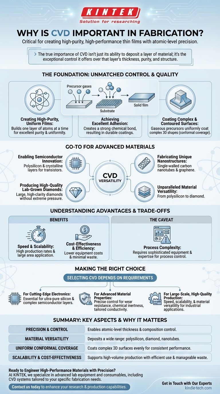
In short, Chemical Vapor Deposition (CVD) is critical to modern fabrication because it provides an unparalleled method for creating high-purity, high-performance thin films with atomic-level precision. This capability is fundamental to manufacturing the most advanced technologies, from the microprocessors in our computers to protective coatings on industrial equipment.
The true importance of CVD isn't just its ability to deposit a layer of material; it's the exceptional control it offers over that layer's thickness, purity, and structure. This control allows us to engineer materials with specific, tailored properties that would be impossible to achieve through other means.
The Foundation of CVD: Unmatched Control and Quality
The power of CVD comes from its unique process, where precursor gases react on a substrate surface to form a solid film. This bottom-up approach is the key to its precision and quality.
Creating High-Purity, Uniform Films
CVD builds materials one layer of atoms at a time. This results in films with excellent purity and uniformity across a surface, which is critical for predictable performance in sensitive applications like electronics.
Achieving Excellent Adhesion
Because the film is formed through chemical reactions directly on the substrate, it creates a strong chemical bond. This results in coatings with excellent adhesion that are far more durable than simple physical coatings.
Coating Complex and Contoured Surfaces
The gaseous nature of the precursors allows CVD to uniformly coat complex, three-dimensional shapes. This "conformal coverage" ensures that even intricate or non-flat components receive a consistent, protective layer.
Why CVD is a Go-To for Advanced Materials
CVD is not a single technique but a versatile platform adaptable to an enormous range of materials and applications, making it indispensable for innovation.
Unparalleled Material Versatility
The process can be used to fabricate a vast array of materials. This includes foundational elements like polysilicon, complex nanostructures like carbon nanotubes, and ultra-hard materials like diamond.
Enabling Semiconductor Innovation
The electronics industry relies heavily on CVD. It's the standard for depositing the polysilicon and intricate crystalline layers that form the basis of transistors and integrated circuits. Specialized techniques like MOCVD are essential for modern semiconducting wafers.
Fabricating Unique Nanostructures
CVD is a fast and effective method for producing advanced nanostructures. It enables the industrial-scale production of single-walled carbon nanotubes and the creation of materials like graphene, a single-atom-thick sheet of carbon with remarkable properties.
Producing High-Quality Lab-Grown Diamonds
The CVD method allows for the growth of large, high-clarity diamonds on various substrates. It achieves this without the extreme pressures required by other methods, often resulting in diamonds with higher clarity and fewer metallic inclusions.
Understanding the Practical Advantages and Trade-offs
While powerful, choosing a fabrication method requires understanding its operational benefits and limitations.
The Benefit of Speed and Scalability
Compared to many other nanofabrication techniques, CVD is a fast and scalable process. It facilitates high production rates and can be applied over large areas, making it commercially viable for everything from solar panels to tool coatings.
Cost-Effectiveness and Efficiency
For many applications, CVD is a cost-effective solution. Equipment costs can be lower than competing high-pressure technologies, and the process generates little waste as most byproducts are gases that are easily managed.
The Caveat: Process Complexity
The primary trade-off for CVD's versatility and precision is process control complexity. Managing precursor gases, high reaction temperatures, and vacuum conditions requires sophisticated equipment and expertise to ensure repeatable, high-quality results.
Making the Right Choice for Your Application
Selecting CVD depends entirely on your material and performance requirements. It is not always the simplest solution, but it is often the best.
- If your primary focus is cutting-edge electronics: CVD is essential for depositing the ultra-pure silicon and complex semiconductor layers that modern microchips demand.
- If your primary focus is advanced material properties: CVD offers precise control over film composition for applications needing extreme wear resistance, chemical inertness, or tailored electrical conductivity.
- If your primary focus is large-scale, high-quality production: The speed, scalability, and material versatility of CVD make it a leading choice for industrial applications from aerospace components to diamond synthesis.
Ultimately, CVD's importance lies in its unique ability to translate atomic-level designs into tangible, high-performance materials at scale.
Summary Table:
| Key Aspect | Why It Matters |
|---|---|
| Precision & Control | Enables atomic-level thickness and composition control for tailored material properties. |
| Material Versatility | Deposits a wide range of materials, from polysilicon to diamond and carbon nanotubes. |
| Uniform Conformal Coverage | Coats complex 3D surfaces evenly, ensuring consistent performance on intricate components. |
| Scalability & Cost-Effectiveness | Supports high-volume production with efficient use of precursors and manageable waste. |
Ready to Engineer High-Performance Materials with Precision?
At KINTEK, we specialize in providing advanced lab equipment and consumables, including CVD systems tailored to your specific fabrication needs. Whether you're developing next-generation semiconductors, creating durable protective coatings, or synthesizing advanced nanomaterials, our expertise ensures you achieve the purity, adhesion, and uniformity critical for success.
Contact us today to discuss how our solutions can enhance your research and production capabilities. Let's build the future of materials science together.
Visual Guide
Related Products
- CVD Diamond Dressing Tools for Precision Applications
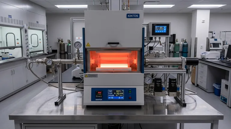
- Multi Heating Zones CVD Tube Furnace Machine Chemical Vapor Deposition Chamber System Equipment
- CVD Diamond Domes for Industrial and Scientific Applications
- CVD Diamond for Thermal Management Applications
- Chemical Vapor Deposition CVD Equipment System Chamber Slide PECVD Tube Furnace with Liquid Gasifier PECVD Machine
People Also Ask
- What color diamonds are CVD? Understanding the Process from Brown Tint to Colorless Beauty
- What is CVD diamond? The Ultimate Guide to Lab-Grown Diamonds and Their Uses
- What is chemical vapor deposition of diamond? Grow High-Purity Diamonds Atom-by-Atom
- What are the disadvantages of CVD diamonds? Understanding the trade-offs for your purchase.
- How do you identify a CVD diamond? The Definitive Guide to Lab-Grown Diamond Verification


