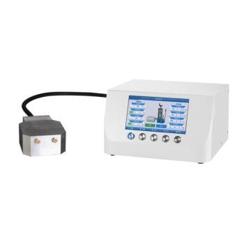
Types of Semiconductor Annealing Processes
Tube Furnace Annealing
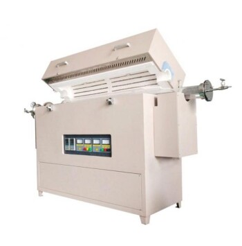
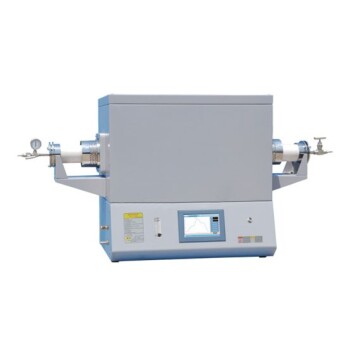
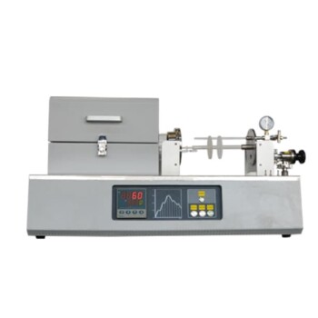
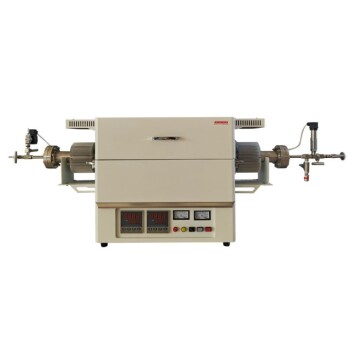
Tube furnace annealing involves placing the material within a cylindrical, closed chamber constructed from high-temperature-resistant materials such as quartz. This chamber is heated using embedded resistance wires, which facilitate uniform temperature distribution and allow for precise control over temperature gradients. This method is particularly well-suited for extended annealing treatments, especially those requiring high temperatures.
The cylindrical cavity of the tube furnace is encircled by heating coils, which are embedded in a thermally insulating matrix. Temperature control is achieved through feedback from a thermocouple, ensuring accurate and stable heating conditions. More sophisticated models may feature multiple heating zones, enabling complex transport experiments where materials are exposed to varying temperatures within the same chamber.
Advanced heating elements, such as molybdenum disilicide (MoSi2), can elevate working temperatures up to 1800 °C, broadening the range of applications. Common materials for the reaction tubes include alumina, Pyrex, and fused quartz, with options like molybdenum or tungsten for handling corrosive materials.
Tube furnaces are extensively used in the synthesis and purification of inorganic compounds, and occasionally in organic synthesis. The ability to maintain uniform temperatures and control thermal gradients makes them ideal for long-duration, high-temperature processes.
RTP Rapid Annealing
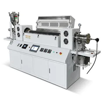
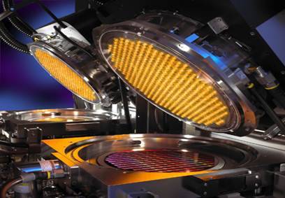
RTP (Rapid Thermal Processing) rapid annealing employs high-intensity light sources, such as infrared lamps, to swiftly elevate wafer temperatures. This method achieves high temperatures within a brief timeframe—ranging from a few seconds to tens of seconds—and can subsequently cool the wafers rapidly. The process meticulously controls the rates of heating and cooling, as well as the precise temperatures and durations, thereby enhancing both the stability and repeatability of the annealing process.
This technique is particularly crucial for rapid heat treatments across various materials, including electronics, ceramics, inorganic substances, metals, and composite materials. The precise temperature control inherent to RTP ensures uniform and consistent results, making it an indispensable tool in industries requiring high-precision thermal treatments.
Laser Annealing
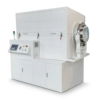
Laser annealing employs a highly focused laser beam to achieve localized heating of materials to extreme temperatures. This process involves directing a laser beam with a precise wavelength and power through a lens, which then scans the target surface. The result is instantaneous, localized heating, making it ideal for applications requiring fine control over thermal treatment.
One of the primary advantages of laser annealing is its ability to precisely target specific areas, which is particularly useful in microelectronic device fabrication. This method is often employed to repair lattice defects and refine patterns in semiconductor manufacturing. By focusing on minute areas, laser annealing ensures that only the intended regions are affected, minimizing thermal damage to surrounding areas.
Compared to other annealing techniques, laser annealing offers unique benefits such as very short localized heating and cooling times, precise control over heating intensity, and the ability to treat single points sequentially. These characteristics make it a valuable tool in industries where fine-tuning and precision are paramount.
Characteristics of Annealing Processes
Number of Treatments
The method of treatment varies significantly among the different semiconductor annealing processes. Tube Furnace Annealing employs batch processing, where multiple wafers are treated simultaneously in a single run. This approach is particularly efficient for large-scale production and long annealing treatments, making it suitable for high-temperature processes that require uniform temperature distribution.
In contrast, RTP (Rapid Thermal Processing) Rapid Annealing offers flexibility in processing, capable of treating either single wafers or multiple chips in one cycle. This method leverages high-intensity light sources, such as infrared lamps, to achieve rapid heating and cooling cycles, which are crucial for maintaining process stability and repeatability. The ability to handle both single and multi-chip processing makes RTP a versatile option for various semiconductor applications.
Laser Annealing, on the other hand, operates on a much more localized scale. It uses a concentrated laser beam to heat individual points sequentially, providing precise control over the heating intensity and location. This method is ideal for microelectronic devices where localized heating is necessary, such as fine patterning and repair of lattice defects. The sequential treatment of single points ensures high precision and minimal thermal impact on surrounding areas.
| Annealing Process | Treatment Method | Suitability |
|---|---|---|
| Tube Furnace Annealing | Batch processing | Large-scale production, high-temperature processes |
| RTP Rapid Annealing | Single or multi-chip | Versatile, rapid heat treatment for electronics and materials |
| Laser Annealing | Single points sequentially | Microelectronic devices, precise localized heating and defect repair |
Rise and Fall Temperature Rate
The rate at which temperature rises and falls during annealing processes varies significantly among different methods. Tube Furnace Annealing involves prolonged heating and cooling cycles, allowing for a gradual and controlled temperature change. This method is particularly suitable for processes that require long durations at high temperatures, ensuring uniform thermal treatment over extended periods.
In contrast, RTP Rapid Annealing employs high-intensity light sources to achieve rapid heating and cooling times, often spanning from a few seconds to tens of seconds. This method offers precise control over the heating and cooling rates, temperatures, and times, which is crucial for maintaining process stability and repeatability. The swift temperature changes are essential for applications in electronics, ceramics, inorganic materials, metals, and composites, where rapid heat treatment is necessary.
Laser Annealing, on the other hand, utilizes a concentrated laser beam to provide very short localized heating and cooling times. The laser beam, with its specific wavelength and power, is focused through a lens and scanned over the target surface, enabling instantaneous localized heating. This method is particularly advantageous for fine patterning and repair of lattice defects in semiconductor manufacturing, as well as for the localized heating and annealing of microelectronic devices.
| Annealing Method | Heating and Cooling Times | Application Focus |
|---|---|---|
| Tube Furnace Annealing | Prolonged | Extended high-temperature processes |
| RTP Rapid Annealing | Short (seconds to tens of seconds) | Rapid heat treatment in various materials |
| Laser Annealing | Very short (localized instantaneous) | Localized heating in semiconductor devices |
Temperature Uniformity
Temperature uniformity is a critical factor in semiconductor annealing processes, influencing the quality and performance of the final product. Each annealing method—Tube Furnace Annealing, RTP Rapid Annealing, and Laser Annealing—offers distinct approaches to achieving temperature consistency.
Tube Furnace Annealing excels in providing a more uniform temperature distribution across the material. This is achieved through the design of the furnace chamber, which is typically made of high-temperature resistant materials like quartz. The chamber is heated by resistance wires, ensuring a controlled and uniform temperature gradient. This method is particularly suitable for long annealing treatments, especially for high-temperature processes, where maintaining a consistent temperature is crucial.
RTP Rapid Annealing focuses on precise control of temperature uniformity and accuracy. By using high-intensity light sources such as infrared lamps, RTP can rapidly heat wafers to high temperatures in a matter of seconds. This rapid heating and cooling capability allow for precise control over the heating and cooling rates, temperatures, and times, enhancing process stability and repeatability. The ability to maintain tight temperature tolerances makes RTP ideal for applications requiring rapid heat treatment in various materials.
Laser Annealing offers very precise control over the heating intensity of single points. This method uses a concentrated laser beam to locally heat the material to high temperatures, allowing for instantaneous and localized heating. The laser beam, with its specific wavelength and power, is focused through a lens and scanned over the target surface, enabling fine patterning and repair of lattice defects in semiconductor manufacturing. The precision of laser annealing is unparalleled, making it an essential tool for microelectronic device fabrication.
| Annealing Method | Temperature Uniformity | Control Precision |
|---|---|---|
| Tube Furnace Annealing | More uniform temperature distribution | Moderate |
| RTP Rapid Annealing | Precise control of uniformity | High |
| Laser Annealing | Very precise control of single points | Highest |
The choice of annealing method depends on the specific requirements of the application, including the need for temperature uniformity, control precision, and the nature of the material being treated.
Thermal Gradient
Thermal gradients play a crucial role in the effectiveness and efficiency of semiconductor annealing processes. Each method—Tube Furnace Annealing, RTP Rapid Annealing, and Laser Annealing—exhibits distinct characteristics in terms of thermal gradients, which significantly influence the quality and precision of the annealing process.
Tube Furnace Annealing maintains small thermal gradients due to its design and operational principles. The material is placed in a long, closed tube-shaped furnace chamber made of high-temperature resistant materials like quartz. The chamber is heated by a resistance wire, ensuring uniform temperature distribution and controlled temperature gradients. This uniformity is particularly beneficial for long annealing treatments, especially for high-temperature processes, where maintaining a consistent thermal environment is essential.
In contrast, RTP Rapid Annealing and Laser Annealing exhibit large thermal gradients. RTP rapidly heats wafers using high-intensity light sources like infrared lamps, reaching high temperatures in a short time (a few seconds to tens of seconds). This rapid heating and cooling process create significant thermal gradients, which are managed through precise control of heating and cooling rates, temperatures, and times. This method is crucial for rapid heat treatment in electronics, ceramics, inorganic, metal, and composite materials, where speed and precision are paramount.
Laser Annealing uses a concentrated laser beam to locally heat the material to high temperatures. A laser beam of specific wavelength and power is focused through a lens and scanned over the target surface for localized instantaneous heating. This method is commonly used for localized heating and annealing of microelectronic devices and for fine patterning and repair of lattice defects in semiconductor manufacturing. The large thermal gradients in Laser Annealing are a direct result of the highly localized and instantaneous nature of the heating process, which requires very precise control of heating intensity of single points.
| Annealing Method | Thermal Gradient Characteristics |
|---|---|
| Tube Furnace Annealing | Small thermal gradients |
| RTP Rapid Annealing | Large thermal gradients |
| Laser Annealing | Large thermal gradients |
Understanding these thermal gradient differences is essential for selecting the appropriate annealing method based on the specific requirements of the semiconductor material and the desired outcome of the annealing process.
Atmosphere Control
Atmosphere control is a critical aspect of semiconductor annealing processes, influencing the quality and consistency of the final product. Each method has its own approach to managing the environment within the annealing chamber.
-
Tube Furnace Annealing: This method faces significant challenges in atmosphere control. The long, closed tube-shaped furnace chamber, while effective for uniform temperature distribution, makes it difficult to maintain precise control over the atmosphere. This limitation can affect the purity and integrity of the annealing process, particularly in high-temperature applications.
-
RTP Rapid Annealing: In contrast, RTP (Rapid Thermal Processing) excels in precise atmosphere control. By utilizing high-intensity light sources, RTP can rapidly heat wafers to high temperatures within seconds. This rapid heating allows for better control over multiple atmospheres and vacuum conditions. The ability to switch between different atmospheres quickly enhances the flexibility and precision of the annealing process, making it ideal for applications requiring rapid heat treatment in various environments.
-
Laser Annealing: Laser annealing offers an even more refined level of atmosphere control. The concentrated laser beam, used for localized heating, can be precisely controlled to manage the atmosphere within the target area. This localized approach enables the use of multiple atmospheres and vacuum conditions, tailored to the specific needs of microelectronic devices and semiconductor manufacturing. The high precision of laser annealing ensures that the thermal treatment is optimized for each point on the material, minimizing defects and improving overall quality.
In summary, while Tube Furnace Annealing struggles with atmosphere control, both RTP Rapid Annealing and Laser Annealing provide advanced capabilities to manage multiple atmospheres and vacuum conditions with high precision.
Cost
When considering the cost of semiconductor annealing processes, it is essential to evaluate both the initial investment and the operational expenses. Tube Furnace Annealing stands out as the most economical option due to its straightforward design and relatively low maintenance requirements. The equipment is typically less expensive to procure and operate, making it an attractive choice for manufacturers with budget constraints.
In contrast, RTP Rapid Annealing and Laser Annealing involve higher initial costs. RTP systems require sophisticated infrared lamp arrays and advanced temperature control mechanisms, which significantly increase the upfront investment. Similarly, Laser Annealing systems demand high-powered laser equipment and precise optical components, further driving up the cost. However, these higher costs are often justified by the enhanced capabilities and efficiency these methods offer, particularly in applications requiring rapid and localized heating.
| Annealing Method | Initial Cost | Operational Cost |
|---|---|---|
| Tube Furnace Annealing | Low | Low |
| RTP Rapid Annealing | High | Moderate |
| Laser Annealing | High | High |
The operational costs for RTP and Laser Annealing are also higher due to the need for continuous maintenance and the consumption of more energy. Despite these higher expenses, the precision and speed of these methods can lead to cost savings in the long run by improving production efficiency and reducing the number of defective products.
In summary, while Tube Furnace Annealing is the most cost-effective option, RTP Rapid Annealing and Laser Annealing offer advanced capabilities that may justify their higher costs in certain high-precision manufacturing scenarios.
Related Products
- Multi-zone Laboratory Tube Furnace
- Vertical Laboratory Tube Furnace
- 1400℃ Laboratory High Temperature Tube Furnace with Alumina Tube
- 1700℃ Laboratory High Temperature Tube Furnace with Alumina Tube
- Vacuum Sealed Continuous Working Rotary Tube Furnace Rotating Tube Furnace

