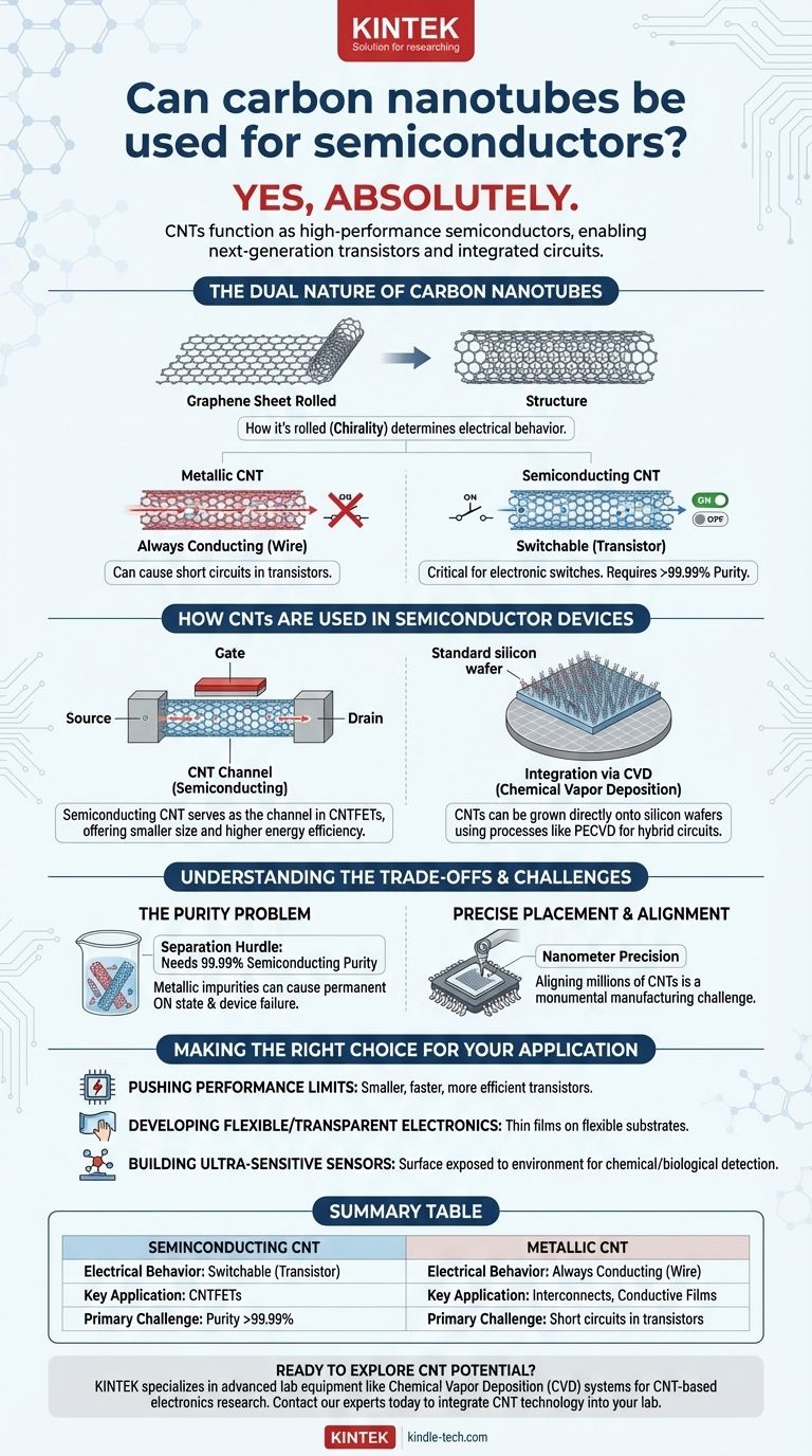
Yes, absolutely. Carbon nanotubes (CNTs) possess remarkable electronic properties that allow them to function as high-performance semiconductors. They are not just a theoretical possibility but are actively being used to build next-generation transistors and integrated circuits that have the potential to outperform traditional silicon-based technology.
The critical factor to understand is that a carbon nanotube's electrical behavior—whether it acts as a semiconductor or a metal—is determined by its specific atomic structure. This dual nature is both the source of its immense potential and the primary challenge in its practical application.
The Dual Nature of Carbon Nanotubes
To understand why CNTs are so promising for semiconductors, you must first grasp their unique structural properties. A CNT is essentially a sheet of graphene, a single layer of carbon atoms, rolled into a seamless cylinder.
Metallic vs. Semiconducting Behavior
How this graphene sheet is "rolled" determines everything. Depending on the angle and diameter of the tube, the CNT will behave either like a metallic wire (always conducting electricity) or a semiconductor (able to switch its conductivity on and off).
The Deciding Factor: Chirality
This structural property is known as chirality. For electronic devices like transistors, which are essentially electrical switches, only the semiconducting type of CNT is useful. A metallic CNT cannot be "turned off" and would create a short circuit.
Why This Is Critical for Electronics
The ability to switch a material from a non-conducting state ("off") to a conducting state ("on") is the fundamental principle of a transistor. Semiconducting CNTs allow this switching at incredibly small scales with high efficiency, which is why they are a target for replacing or augmenting silicon.
How CNTs Are Used in Semiconductor Devices
The primary application for semiconducting CNTs is in building a new class of transistors, often seen as the successor to the silicon-based MOSFET.
Building CNT Field-Effect Transistors (CNTFETs)
A semiconducting carbon nanotube can serve as the channel in a Field-Effect Transistor (FET). In this device, a voltage applied to a "gate" controls the flow of current through the nanotube, turning the transistor on or off. These CNTFETs have demonstrated capabilities for being smaller and more energy-efficient than their silicon counterparts.
Integration with Existing Technology
A key advantage is that CNTs can be integrated with traditional microelectronics manufacturing. As noted in research, processes like plasma-enhanced chemical vapor deposition (PECVD) can be used to deposit CNTs directly onto standard silicon wafers.
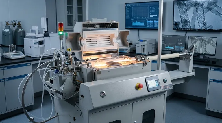
Manufacturing with Chemical Vapor Deposition (CVD)
CVD is a cornerstone of the modern semiconductor industry. This process "grows" thin films of material onto a substrate. Using this established technique allows for the creation of hybrid circuits that combine the strengths of both silicon and carbon nanotubes on a single chip.
Understanding the Trade-offs and Challenges
While the potential of CNTs is immense, significant engineering challenges have slowed their widespread commercial adoption. These are not scientific curiosities but hard manufacturing problems that the industry is actively working to solve.
The Purity Problem
The single greatest hurdle is separation. When CNTs are synthesized, the process typically creates a random mix of both semiconducting and metallic types. For building reliable integrated circuits, a purity of over 99.99% semiconducting CNTs is required.
The Impact of Metallic Impurities
Even a tiny fraction of metallic CNTs in a transistor channel can be disastrous. A single metallic tube can act as a permanent "on" switch, preventing the transistor from ever turning off completely. This leads to massive power leakage and device failure.
Precise Placement and Alignment
Beyond just creating pure semiconducting CNTs, they must be placed with nanometer precision on the chip to form the desired circuit. Aligning millions or billions of these tiny tubes in the correct orientation is a monumental manufacturing challenge.
Making the Right Choice for Your Application
Carbon nanotubes are not a universal replacement for silicon but a specialized material that unlocks new capabilities. The decision to explore CNTs depends entirely on your ultimate goal.
- If your primary focus is pushing the limits of performance and energy efficiency: CNTs offer a path to creating transistors that are smaller and faster than what is possible with silicon, leading to more powerful and efficient processors.
- If your primary focus is developing flexible or transparent electronics: CNTs can be deposited as a thin film on flexible plastic or transparent glass substrates, enabling applications like wearable sensors and transparent displays that are impossible with rigid silicon wafers.
- If your primary focus is building ultra-sensitive sensors: The entire surface of a CNT is exposed to its environment, making it exquisitely sensitive to nearby molecules, which is ideal for advanced chemical and biological sensors.
Ultimately, carbon nanotubes represent a fundamental shift from engineering a bulk material like silicon to designing electronics at the molecular level.
Summary Table:
| Property | Semiconducting CNT | Metallic CNT |
|---|---|---|
| Electrical Behavior | Can be switched on/off (transistor) | Always conducting (wire) |
| Key Application | Building CNT Field-Effect Transistors (CNTFETs) | Interconnects, conductive films |
| Primary Challenge | Requires >99.99% purity for reliable circuits | Can cause short circuits if present in transistors |
Ready to explore the potential of carbon nanotubes for your semiconductor or sensor applications?
KINTEK specializes in providing the advanced lab equipment and consumables, such as Chemical Vapor Deposition (CVD) systems, essential for researching and developing next-generation CNT-based electronics. Our expertise supports your work in creating high-performance, energy-efficient devices.
Contact our experts today to discuss how we can help you integrate CNT technology into your laboratory.
Visual Guide
Related Products
- Customizable PTFE Wafer Carriers for Semiconductor and Lab Applications
- Versatile PTFE Solutions for Semiconductor and Medical Wafer Processing
- Hexagonal Boron Nitride HBN Thermocouple Protection Tube
- Boron Nitride (BN) Ceramic Tube
- Conductive Carbon Cloth Carbon Paper Carbon Felt for Electrodes and Batteries
People Also Ask
- Are semiconductors thin or thick? Discover the Power of Microscopic Thinness in Modern Electronics
- Why is slender PTFE tubing necessary for flow control in multi-channel catalyst aging? Ensure Equal Gas Distribution
- How is PTFE utilized for insulation in Alloy 22 corrosion setups? Ensure Signal Purity & Accuracy
- Why is PTFE wire used for hanging metal specimens in biodiesel corrosion tests? Ensure Pure Experimental Results
- What are the specific applications of PTFE in micro-batch slug flow systems? Enhance Your Microfluidic Reaction Purity