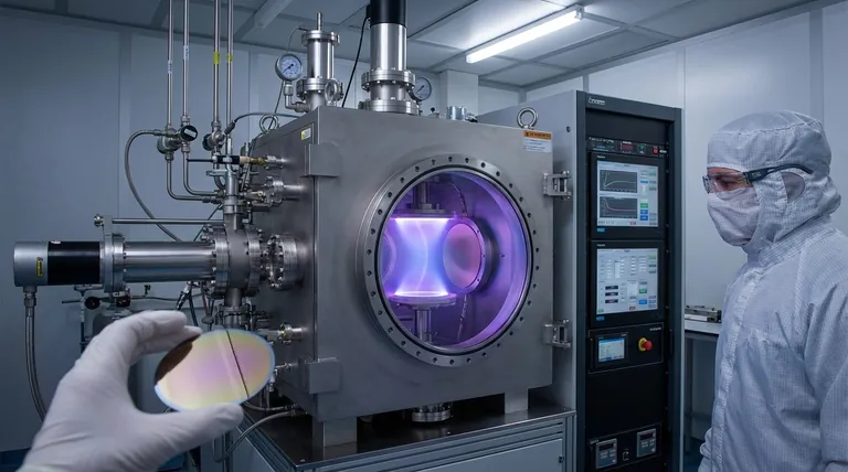
The primary advantage of RF magnetron sputtering is its unique ability to deposit high-quality thin films from virtually any material, including electrical insulators like oxides and nitrides. Unlike its direct current (DC) counterpart, the alternating nature of the radio frequency (RF) power source prevents electrical charge from building up on the target material, which eliminates destructive arcing and enables stable, efficient deposition.
The core reason to choose RF magnetron sputtering is its unmatched versatility. It solves the fundamental problem of sputtering non-conductive materials, opening the door to depositing a vast range of advanced dielectrics, semiconductors, and composites with high quality and process stability.
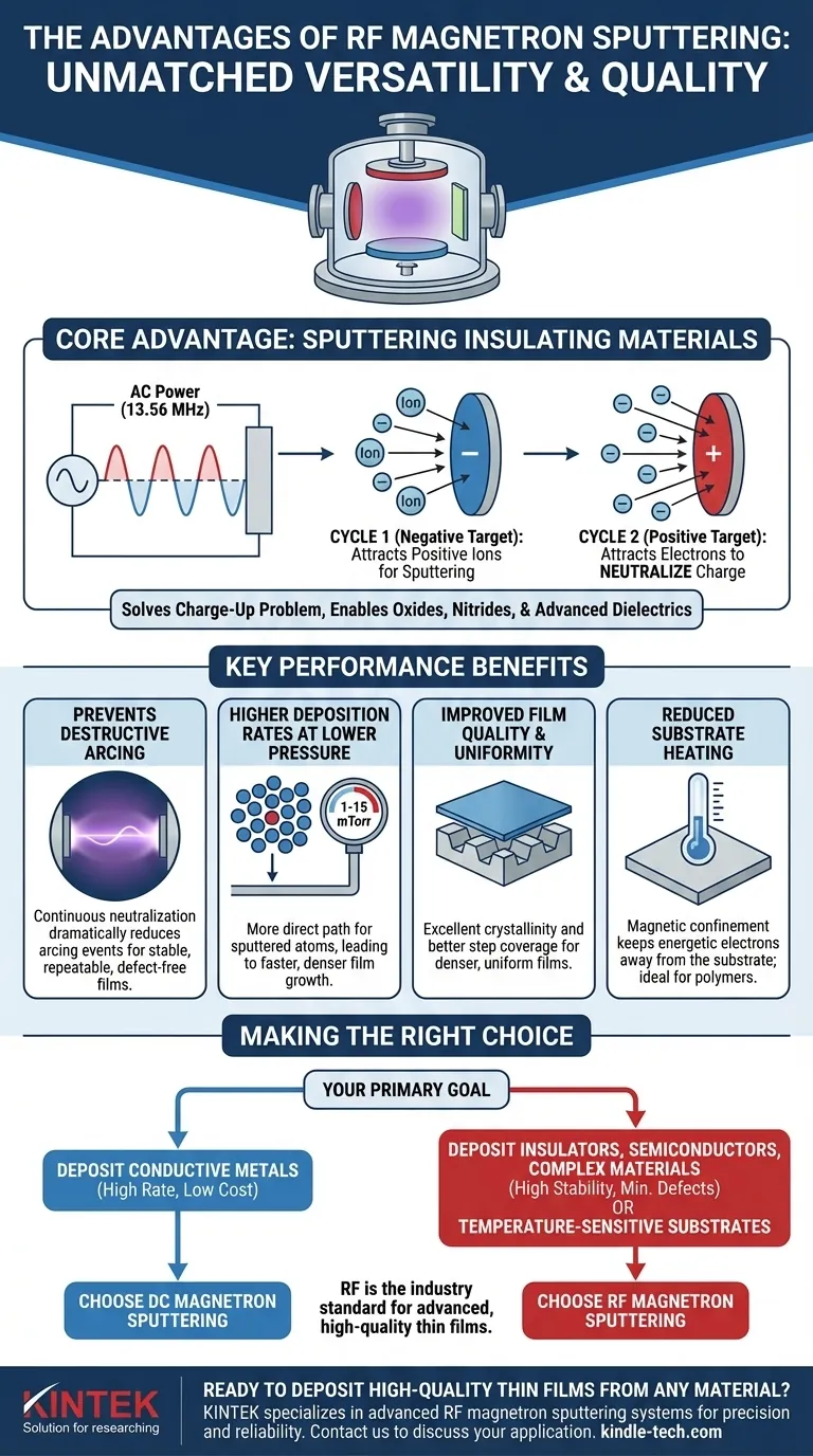
The Core Advantage: Sputtering Insulating Materials
The defining capability of RF sputtering is its ability to handle electrically insulating targets, a task impossible for simpler DC sputtering systems. This is a direct consequence of how RF power interacts with the plasma and the target material.
How RF Power Solves the Charge-Up Problem
In any sputtering process, the target is bombarded by positive ions from the plasma. When sputtering a conductive material with DC power, this positive charge is neutralized by the target's free electrons.
With an insulating target, however, this positive charge cannot dissipate. This "charge-up" effect quickly repels the positive plasma ions, extinguishing the sputtering process entirely.
RF sputtering solves this by using an AC power source, typically at 13.56 MHz. During one half of the cycle, the target is negative, attracting ions for sputtering. During the other half, it becomes positive, attracting electrons from the plasma which neutralize the accumulated positive charge from the previous cycle.
Preventing Destructive Arcing
The buildup of localized positive charge on an insulating target surface is a primary cause of arcing. These are uncontrolled, high-current electrical discharges that can damage the target, contaminate the film, and destabilize the entire process.
By continuously neutralizing the surface charge every cycle, RF sputtering dramatically reduces arcing events. This leads to a much more stable and repeatable deposition process, which is critical for producing high-quality, defect-free films.
Enhancing Deposition Performance and Quality
Beyond its material versatility, RF sputtering provides several key performance benefits that lead to higher quality films and more efficient processes.
Higher Deposition Rates at Lower Pressure
RF fields are highly efficient at energizing electrons, allowing a stable plasma to be sustained at much lower pressures (e.g., 1-15 mTorr) compared to DC sputtering.
Operating at lower pressure means there are fewer gas atoms between the target and the substrate. Sputtered atoms therefore travel a more direct path, resulting in higher deposition rates and a denser film structure.
When combined with a magnetic field (magnetron sputtering), electrons are trapped near the target surface, further increasing plasma density and boosting the sputtering rate significantly.
Improved Film Quality and Uniformity
The low-pressure environment of RF sputtering reduces the chance of sputtered atoms colliding with gas molecules. This preserves their kinetic energy until they impact the substrate, promoting the growth of denser, more uniform films with excellent crystallinity.
This process also provides better step coverage—the ability to coat the sides and bottoms of microscopic features on a substrate—compared to techniques like thermal evaporation.
Reduced Substrate Heating
In RF magnetron systems, the magnetic field confines the highly energetic electrons to a region near the target. This prevents them from bombarding and excessively heating the substrate, which is a critical advantage when depositing films on temperature-sensitive materials like polymers.
Understanding the Trade-offs
While powerful, RF sputtering is not without its considerations. Understanding its trade-offs is key to making an informed decision.
RF vs. DC Sputtering
The choice is straightforward: if your target is a conductive metal, DC magnetron sputtering is often simpler, cheaper, and offers very high rates. If your target is an insulator, semiconductor, or composite, RF sputtering is the necessary and superior choice.
System Complexity and Cost
RF sputtering systems are inherently more complex than their DC counterparts. They require an RF power generator, a coaxial cable, and an impedance matching network. This "matchbox" is a critical component that ensures maximum power is transferred to the plasma, but it adds cost and a layer of process complexity.
Recent Developments: RF Diode Sputtering
Modern advancements like RF Diode sputtering can eliminate the need for magnetic confinement. This technology promises even flatter target erosion (no "racetrack" effect), superior coating uniformity, and an even more stable process with minimal arcing, further refining the benefits of the RF approach.
Making the Right Choice for Your Application
To determine if RF magnetron sputtering is the right fit, consider your primary goal.
- If your primary focus is depositing insulating or dielectric films (e.g., SiO₂, Al₂O₃, PZT): RF sputtering is the industry-standard and often the only viable sputtering technique.
- If your primary focus is achieving high process stability and minimal defects with complex materials: The arc-suppression capability of RF sputtering is a decisive advantage.
- If your primary focus is depositing simple metallic films at the lowest cost: A dedicated DC sputtering system may be a more economical solution.
- If your primary focus is coating temperature-sensitive substrates: RF magnetron sputtering's reduced substrate heating makes it a strong candidate.
Ultimately, RF magnetron sputtering provides a robust and versatile platform for depositing the advanced materials that underpin modern technology.
Summary Table:
| Key Advantage | Benefit |
|---|---|
| Sputters Insulating Materials | Enables deposition of oxides, nitrides, and other dielectrics impossible with DC sputtering. |
| Prevents Arcing & Charge Buildup | AC power neutralizes surface charge, ensuring a stable, high-quality deposition process. |
| Higher Deposition Rates at Lower Pressure | Achieves faster, denser film growth compared to other techniques. |
| Improved Film Quality & Uniformity | Produces dense, uniform films with excellent crystallinity and step coverage. |
| Reduced Substrate Heating | Ideal for temperature-sensitive substrates like polymers. |
Ready to deposit high-quality thin films from any material?
KINTEK specializes in advanced lab equipment, including RF magnetron sputtering systems designed for precision and reliability. Whether you are working with insulating dielectrics, semiconductors, or temperature-sensitive substrates, our solutions deliver the process stability and superior film quality you need.
Contact us today using the form below to discuss how our sputtering technology can advance your research and development. Let our experts help you choose the perfect system for your specific application.
Visual Guide
Related Products
People Also Ask
- What is an example of PECVD? RF-PECVD for High-Quality Thin Film Deposition
- What is plasma chemical vapor deposition? A Low-Temperature Thin Film Coating Solution
- What is the role of RF-PECVD in VFG preparation? Mastering Vertical Growth and Surface Functionality
- Why is a Matching Network Indispensable in RF-PECVD for Siloxane Films? Ensure Stable Plasma and Uniform Deposition
- What is plasma enhanced chemical vapour deposition PECVD used for? Enable Low-Temp Thin Films for Electronics & Solar
